Characteristics and Applications of ASK Transmitter Circuit MICRF102
**1 Overview**
The MICRF102 is a single-chip UHF band ASK transmitter IC developed by Micrel Semiconductor, designed for wireless communication applications. It leverages the company’s QwikRadio™ technology to enable seamless "data in, antenna out" functionality. This innovative design allows the chip to automatically perform internal antenna tuning, eliminating the need for manual adjustments and significantly reducing development and production costs.
The MICRF102 operates across a wide range of UHF free frequency bands and is fully compatible with various ASK/OOK (Amplitude Shift Keying/On-Off Keying) receiving modes. It supports data rates from 100 bps up to 20 kbps, making it ideal for a variety of remote control and RF data link systems. When paired with Micrel’s QwikRadio™ receiver circuits, the MICRF102 offers an ultra-low-cost and highly reliable solution for wireless communication systems.
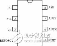
*Figure 1: MICRF102 pinout*
**2 Main Features**
(1) Complete UHF band monolithic transmitter circuit
(2) Transmission frequency range: 300 MHz to 470 MHz
(3) Maximum modulation data rate: 20 kbps
(4) Built-in automatic antenna tuning
(5) Minimal external pin count
(6) Ultra-low quiescent current: <0.04 μA
(7) Encapsulated in an 8-pin SOIC package (4.8 mm × 3.9 mm × 1.6 mm)
**3 Pin Arrangement**
The pin configuration of the MICRF102 is illustrated in Figure 1.
**4 Block Diagram**
Figure 2 provides a detailed block diagram of the MICRF102.
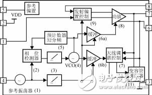
*Figure 2: Block diagram of MICRF102*
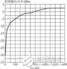
*Figure 3: Relationship between RF output power and PC pin voltage*
**Table 1: PIN Function and Symbol of MICRF102**
| Pin Number | Symbol | Pin Function |
|------------|--------|--------------|
| 1 | PC | RF output power control terminal |
| 2 | VDD | Power positive input |
| 3 | VSS | Power ground |
| 4 | REFOSC | Reference oscillation frequency input |
| 5 | STBY | Transmit mode control terminal; connects to VDD for transmit mode, VSS for standby mode |
| 6 | ANTP | RF power output positive terminal, drives the high end of the loop antenna |
| 7 | ANTM | RF power output negative terminal, drives the low end of the loop antenna |
| 8 | ASK | Amplitude shift keying modulation data input; connect to VDD for equal amplitude mode |
In the block diagram shown in Figure 2, pins 1 through 5 form a UHF frequency synthesizer that generates the carrier frequency required for transmission. The in-phase signal (I) drives the power amplifier, while the quadrature path (Q) compares with the phase of the antenna signal to tune the antenna. The power control unit senses the antenna signal and adjusts the bias current of the power amplifier to regulate the transmit power. An external PCB loop antenna connected to the ANTP and ANTM terminals forms an LC parallel resonant circuit.
**5 Electrical Performance Parameters**
**5.1 Absolute Maximum Ratings**
YIWU JUHE TRADING COMPANY , https://www.nx-vapes.com