A new generation of system design that makes package and PCB design easier
In most cases, modern electronic system design involves designing various components or systems that are relatively isolated from each other. The design of the IC and the pin output are determined by the location of the circuit on the chip. The package designer uses a "throw wall" chip design and designs as short a package bond wire as possible to make the package as small as possible. Then the PCB designer, who has been complaining about it, picks up the packaged IC and racks his brain to find out how to route the signal, which always seems to be mistaken on a pin or solder ball.
With the increasing sophistication of SoCs today and the development of multi-chip packages, companies are beginning to recognize the value of cross-field collaboration between ICs, package substrates, and PCB design groups. Because of the cost sensitivity of high pin count devices, engineers have to rethink how to plan and optimize the I/O layout of the chip while compromising complex IC package variables. And do all of this for multiple board-level platforms. Now, the emergence of various tools has made packaging and PCB design a collaborative and mutually beneficial process.
Cognitive design
To get the most out of it, EDA tools should be aware of the tools that will be used in other processes. There is little mutual understanding in the field of packaging and PCB design. It is true that the FPGA pin output can be defined by the user within a certain range, but "standard" components generally do not have such an option.
By making the tool clear design and product design to other parts of the process, these tools can work together and deliver better system designs in less time. In addition, standard IC chips can be packaged in different ways, depending on the form factor of the end product, resulting in a more optimized solution for various ways.
How do tools quickly recognize each other and then work together to deliver a better design? The design of smartphones and tablets using the same CPU chip is a perfect illustration of this mode. Clearly, many mobile device companies are making such an attempt.
However, compared to smartphones, the available area on the PCB's PCB substrate is significantly larger and has fewer constraints. As a result, the CPU package on the tablet may be larger, have different pin outputs, or may consume more power than the CPU on the smartphone. Therefore, a single "standard" package may not be the best application package (Figure 1).
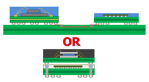
Figure 1: The tablet design may have more available substrate area layout CPU and glue circuitry to allow the upper package to operate. But for smartphones that use the same CPU, this approach is too space-intensive, so a better solution is to use the underlying package.
Now, with the new tools, designers can configure the chip to “see†the design from a package perspective, then move to the PCB (traditional method), or first understand the PCB design requirements and then return to the package design. Moreover, they can get every product that uses the CPU, and then go back from the PCB to design the best package optimized for this design.
From a packaging perspective, physical design rules are determined by PCB design requirements. The tool then interacts with the rules and package designer to deliver the best package for the specific application of the chip. This relatively fast package design approach also explores different ideas to quickly find the best solution.
real case scenario
Figure 2 shows the hypothetical product design. In this example, the shape parameters of the final product are known and the components have been initially laid out. Note the description at the top, where the layout CPU has been reserved. Using this input, the tool can begin a path lookup, experimenting with multiple package configurations based on rules written by PCB designers and package designers.
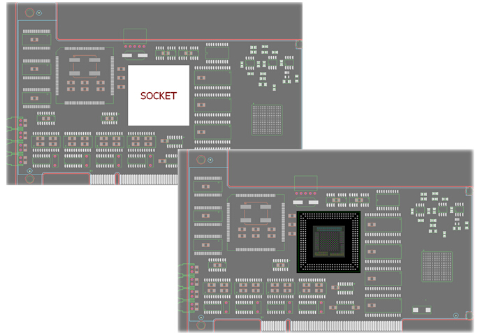
Figure 2: In general, physical shape parameters are the main constraints of product design. Using path-finding tools, package and PCB designers can collaborate to find the best package within physical design constraints and simplify fan-out and routing of complex packages.
For each design, traditional routing can be done on the PCB to determine the optimal package and pinout. The rules allow the designer to define various parameters, such as unused output corner pins, methods for connecting differential pairs, methods for distributing power and ground, and methods for processing data and address buses.
Once the rules are determined, it's not just "press the button and sit back", but rather more direct, faster, and more accurate than using spreadsheets and pin lists, which is the status quo.
advantage
Tool cognitive design has significant advantages and can be optimized for design in any design area. First, it makes it easier to customize multiple package designs to make optimal use of a given component in accordance with the required form factor. Then look at the design from multiple “what-if†scenarios, such as smaller packages, lower cost, simplest fanouts, and exits. Second, because of the large number of pins, the use of spreadsheets and pin lists for package design is not enough. When hundreds of pin data are manually entered, the error rate is almost 100%. Of course, its advantages include: improved quality, optimal packaging for shape parameters, reduced errors, and significant time savings throughout the system design.
Uvc Lamp,Uv Germicidal Bulb,Uv Germicidal Lamp,Uvc Tube
Changxing leboom lighting product CO.Ltd. , https://www.leboomuv.com