What is the application of MOSFETs into the field of IGBT applications?
Broadly speaking, this assumption is correct: MOSFETs support faster switching speeds and higher efficiency, but are less durable and have lower maximum current ratings. The IGBT has a slower switching speed, higher switching losses and conduction losses, but it is more durable and can handle higher peak currents and continuous current values.
The general rule for choosing a MOSFET or IGBT is constant, and for most applications it is obvious to choose which device is more suitable. But in fact, these two types of devices are constantly evolving due to constant product and technology development by major suppliers such as STMicroelectronics, ON Semiconductor and Fairchild Semiconductor.
By explaining the operating characteristics of the latest generation of MOSFETs and IGBTs, this article enables users to better understand the most suitable device type that best meets the application requirements and explains the gray areas of current power transistor selection.
Speed ​​and efficiency
The development of IGBTs and MOSFETs is largely aimed at increasing switching speed and efficiency by reducing switching losses and conduction losses.
In bipolar transistors, the method focuses on improving its relatively slow turn-off characteristics, which causes a large "current tail" of the device. In addition, manufacturers of IGBTs are working to reduce the collector-emitter saturation voltage VCE(sat), which determines the on-state voltage of the device, which determines the conduction loss.
Another problem with some of the early IGBT types was their negative temperature coefficient, which could cause thermal runaway: it was difficult to run multiple devices simultaneously, failing to provide high power output.
The development of the following three technologies provides solutions to this problem: first, punch-through (PT) plane technology, second, non-punch-through (NPT) plane, third, today's IGBT trench gate field termination technology, such as Figure 1 shows.
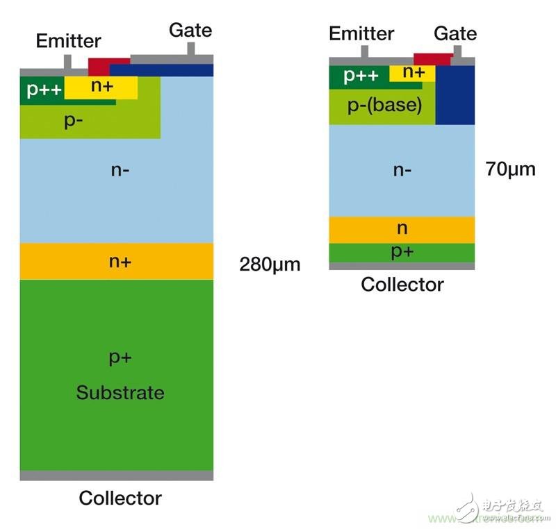
Figure 1: Comparison of the structure of planar (left) and trench gate-off IGBTs (right) (Source: STMicroelectronics)
These wafer fabrication techniques enable manufacturers to continuously reduce the quality of silicon in their devices. Its advantages include:
Reduced unit cost because each wafer can be cut into more devices
Achieve faster switching speeds
Shorten the length of the current tail for lower switching losses
Reduced collector-emitter saturation voltage
Reduced power consumption enables increased power density, so today's IGBTs can handle 50% higher average current than first-generation IGBTs. The devices benefiting from the latest IGBT technology are shown in Table 1.
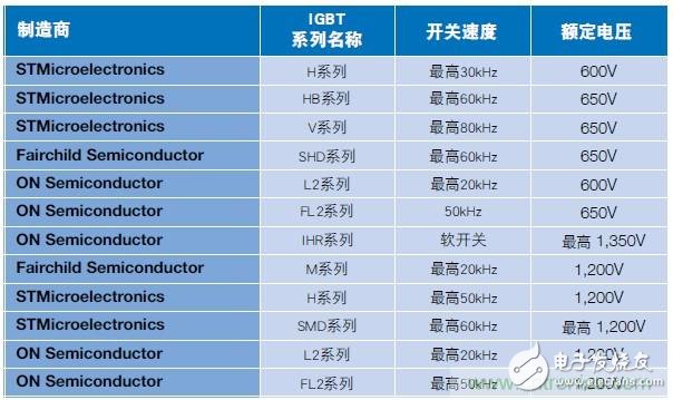
Table 1: The latest series of IGBTs offer low loss and high switching speed
MOSFET technology: lower on-resistance
Like IGBTs, MOSFETs have undergone many evolutions over the past two decades.
In the early days, the structure of the MOSFET was planar: newer MOSFETs benefited greatly from the significant advances in trench gate technology and the introduction of vertical superjunctions. In these new technologies, the gate pins are embedded deeper into the silicon material, enabling better use of existing silicon.
Therefore, even though planar devices are still on the market, trench technology has become the preferred structure for MOSFETs.
The reason that planar MOSFETs are still in use is that comparison with trench gate MOSFETs shows that planar devices have excellent forward bias safe operating area (FBSOA) and non-embedded inductive switching (UIS) avalanche capability. However, these studies also show that the reverse recovery performance of the body diode of the trench MOSFET (characterized by reverse current density) is superior to the equivalent planar MOSFET, as shown in Figure 2.
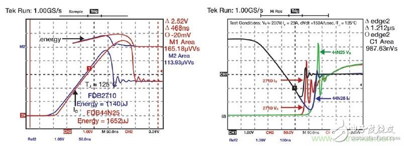
Figure 2: Performance comparison of a planar MOSFET (FDB44N25) with a similar device using trench gate technology (FDB2710) during turn-on (left) and turn-off (right) reverse recovery. (Source: Fairchild Semiconductor)
This is mainly because the structure of a planar MOSFET requires more silicon material, a larger thickness, and a larger contact surface than a trench MOSFET.
This means that when choosing a MOSFET for a specific application, system designers should pay special attention to:
Parasitic parameters of its circuit
Thermal properties of the operating environment
Relative durability and vulnerability of their chosen MOSFET technology
The most important parasitic parameter to consider is the two stray inductances.
The first is the inductor connected in series to the source pin. This inductor is present in the gate drive control loop and acts as a feedback to slow down the gate drive signal. Designers need to be careful not to exceed the gate-source maximum voltage rating.
The second inductor is the inductor connected in series to the drain pin. If not clamped, it will cause an overvoltage spike when the device is turned off. Buffers or clamp devices can be used to minimize this effect. In addition, when turned on, another effect of this inductor is the drain voltage drop, which causes the Miller capacitor to discharge, causing the gate driver to sink more current and achieve a slower overall commutation transition, as shown in Figure 3.
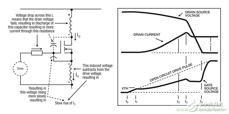
Figure 3: Effect of source stray inductance on turn-on
In order to reduce these effects, the stray circuit inductance must be minimized.
Find the boundary between MOSFET and IGBT applications
As indicated above, the characteristics of IGBTs and MOSFETs make their choice simple in most applications. But at the intersection of features, both device types have their advantages and disadvantages, making selection less easy. The development of MOSFETs based on silicon carbide (SiC) technology has made the choices even more complicated because they offer higher performance (faster switching speeds, lower losses) than silicon MOSFETs, but the unit cost is significantly higher. Today, after many of the above evolutions of IGBT and MOSFET technology, this crossover involves applications with operating voltages above 250V, switching frequencies between 10kHz and 200kHz, and powers exceeding 500W, as shown in Figures 4 and 5.
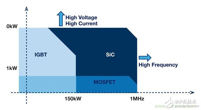
Figure 4: Functional advantages of MOSFETs and IGBTs
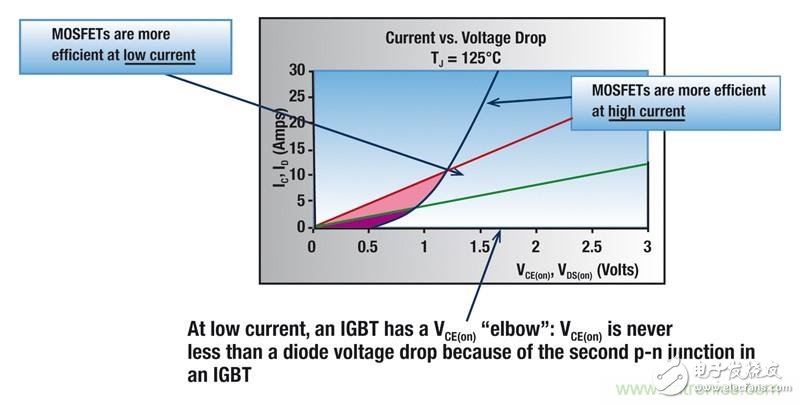
Figure 5: Typical Efficiency & Current Product of IGBTs and MOSFETs
The MOSFET's structure includes a diode that is ideal for handling freewheeling currents. In MOSFETs with voltages below 200V, such as ST's STM F7 series, Fairchild's Power Trench series, NXP's PowerMOS Trench 9 and Trench series, and Vishay's fourth-generation series, their integrated diode switching speeds very fast. To achieve the same functionality as an IGBT, designers must specify a “co-packaged IGBTâ€â€”that is, integrate discrete fast diodes and IGBTs in a single package—a larger, more expensive solution than standard MOSFETs.
In applications with operating voltages above 500V, the choice becomes more complicated: the development of Super Junction (SJ) MOSFETs for high voltage systems with operating voltages exceeding 500V, such as STMicroelectronics' MDmesh II, MDmesh V, FDmesh II and SuperMESH 5 series Fairchild's SuperFet II, Easy Drive, Fast and Fast Recovery (FRFET) series, as well as Vishay's E and EF series. Compared to conventional MOSFETs, SJ MOSFETs can be used as a replacement for "co-packaged IGBTs" in higher voltage ranges. The problem is that the internal body diode of the SJ MOSFET is inherently slower than the IGBT's common FRED packaged ultrafast diode.
When necessary, for example in a half-bridge phase shift topology, a special SJ MOSFET including a relatively fast body diode can be selected. Each of these large MOSFET manufacturers offers these special high-speed SJ MOSFETs, such as STMicroelectronics' FDmesh II or Fairchild's SuperFET II series, but even these devices will never be as fast as ultrafast diodes in standard IGBTs.
At high voltages, SJ MOSFETs are suitable for relatively low power outputs. When operating above 600V and producing high power output, IGBT is still the only option. This is because the saturation voltage of the IGBT is almost constant over the entire current range, and the voltage drop caused by the on-resistance of the MOSFET increases as the current increases. Therefore, at high power levels, the conduction loss of the IGBT is significantly lower than that of the MOSFET.
With a voltage below 600V and a relatively low power output, the MOSFET supports a higher switching speed than the IGBT, providing higher efficiency, making it a more viable option than ever. However, of course, after considering all the performance parameters, the most important engineering parameters may determine the final choice, which is undoubtedly the unit cost.
we offer a wide selection of traffic Steel Pole structures in standard and custom designs.
Yixing Futao Metal Structural Unit Co. Ltd. is com manded of Jiangsu Futao Group.
Traffic Signal Pole, Traffic Light Pole, Led Traffic Signals, Solar Traffic Signal Pole,Traffic Steel Pole
YIXING FUTAO METAL STRUCTURAL UNIT CO.,LTD( YIXING HONGSHENGYUAN ELECTRIC POWER FACILITIES CO.,LTD.) , https://www.chinasteelpole.com