Noise analysis of CCD imaging device
1 Concept and classification of CCD imaging devices
The charge-coupled device is a new type of metal-oxide-semiconductor device. Its basic structure is a close-packed MOS capacitor, which can store the light information charge excited by the incident light in the CCD image sensitive unit and can be properly Driven by the phase sequence clock pulse, the stored charges are transferred in the form of charge packets to achieve self-scanning and complete the conversion from optical signals to electrical signals. Usually this electrical signal is a video signal that conforms to the TV standard. It can be restored to a visible light image of an object on the TV screen, and the signal can also be stored in a tape drive or input into a computer for image enhancement, recognition, storage and other processing. Therefore, the CCD device is an ideal imaging device.
Ordinary scientific CCD devices have limited detection capabilities under low light, and are not suitable for low light imaging. With the development of photoelectric imaging technology, the following low-light CCD imaging devices have emerged: enhanced CCD (ICCD), electron bombardment CCD (EBCCD) and electron multiplying CCD (EMCCD).
2 Noise analysis of CCD imaging device
Charge coupled device (CCD) has been widely used in scientific imaging. It has the following advantages in imaging:
(1) It has higher and wider quantum efficiency than other available detectors;
(2) Very high resolution determined only by pixel size;
(3) Actually, there is no crosstalk and resolution defects like halo.
But no matter what kind of situation, the signal appears always accompanied by noise, of course, using CCD imaging coupling device is no exception. Noise is an important factor in determining image quality.
The output signal of the CCD image sensor is a discrete analog signal sampled in space, which is mixed with various noises and interference, and the noise will affect the ability of the CCD imaging device to detect weak light.
For optoelectronic devices, whether they can detect radiation power small enough is a crucial issue. Therefore, the minimum detectable radiation power is generally listed as an important parameter of all photoelectric detection devices. Pmin is defined as the incident radiation power of the detector when the output signal voltage is equal to the rms value of the output noise voltage. Therefore, the available incident radiation power is:
Where: P is the incident radiation power; un is the mean square value of the noise voltage; Us is the output signal voltage; Pmin is the minimum detectable power. The smaller the Pmin, the stronger the detection capability of the device, that is, the ability to detect weak light. It can be known from equation (1) that under the condition that the output signal voltage is constant, the smaller the noise un, the smaller the Pmin. The device's ability to detect faint light is also stronger. Therefore, the purpose of processing the CCD signal is to eliminate noise and interference as much as possible without losing image details, so as to improve the signal-to-noise ratio and obtain high-quality images. To this end, we must understand the types and characteristics of CCD noise, and carry out corresponding denoising treatment for various noises. Therefore, the study of the noise part of the CCD imaging device is helpful to improve the resolution of the CCD imaging device and also improve the ability to detect weak light. 2.1 Transfer noise
When a charge packet is transferred from one potential well to another, due to various reasons, some charge will be obtained from the previous charge packet, and at the same time some charge will be left behind the latter charge packet. The amount of these charges is random, so there will be fluctuations, which constitute noise. Considering that each transfer includes two processes of obtaining charge and losing charge, the fluctuation noise should be taken as the sum of the two. If there is a complete charge transfer model, the gains and losses are equal, so the noise is twice that of a single process. When Nε << 1, the fluctuations in each transfer process are independent, then the fluctuation noise of N transfers is:
Where: Ns is the number of signal carriers in each charge packet; Ns0 is the number of base carriers in each charge packet.
2.2 Reset noise
The reset noise is the voltage caused by the switch intervening in the capacitor. When the switch is turned OFF, the noise appears, which is also the noise that must occur in the sampling circuit. Even for a CCD image sensor, the FD power supply voltage must be reset before the signal charge is detected. After the reset, the reference FD power supply voltage is restored and noise kTC is added.
After the diode outputs a signal, in order to continuously receive the next charge packet, its voltage needs to be reset. The reset circuit formed by MOST must feed noise into the output circuit during operation. This noise, the reset noise, can be eliminated by correlated double sampling. The reset process can be viewed as a photoelectric process of the capacitor C through the resistor R.
The noise generated by QC (t) is:
2.3 Shot noise
Even if the light intensity is constant, since the light has the particle characteristics of photons, the light incident on the photodiode within a storage time will not have the same number of photons each time. Such a variable characteristic causes light shot noise. The light shot noise is the same as the dark current shot noise, and the square root of the number of photons Ns entering the photodiode is taken as the light shot noise Nn. For example, assuming that light intensity causes 10 000 signal charges in a photodiode, 100 light shot noises occur, and the signal-to-noise ratio is 40 dB.
In general, the shot noise formula of the device is as follows:
According to equation (4), it can be concluded that the most direct way to increase shot noise and make it the main source of noise is to increase the electronic gain G.
2.4 Dark current noise
For CCD image sensors, the cause of dark spots, white damage, or particles is due to the dark current of the photodiode, which is also the most important factor in determining image quality. The cause of fixed image noise is the uneven dark current in each pixel, even if there is no incident light, it is proportional to the storage time of the noise signal voltage, and has a property that is closely related to temperature, as shown in equation (5):
It can be seen from equation (5) that the magnitude of dark current noise is closely related to temperature. In addition, it is also related to the length of time the point packet is stored in the potential well. The longer the storage time, the greater the dark current noise.
3 The method of suppressing the noise of CCD image sensor
When analyzing image quality, the signal-to-noise ratio should be considered. The higher the signal-to-noise ratio, the better the image quality. Therefore, a comprehensive evaluation of the signal-to-noise ratio that determines the performance of the CCD image sensor must be performed.
First of all, once the photographic conditions are changed, some will become more obvious with different types of noise, and some will appear to be replaced in size. Considering the temperature in photography conditions, in general, random noise is proportional to the square root of absolute temperature; on the other hand, in fixed image noise, for every 10 ° C increase in temperature, dark current noise will increase by a factor of two, which is very Strong temperature dependence. Therefore, lowering the temperature can reduce random noise and dark current noise.
In addition, considering the relationship of light intensity, the shot noise of light is proportional to the square root of the amount of signal charge. As the light intensity increases, the signal-to-noise ratio becomes larger, and the dark current is proportional to the storage time of the signal. The longer the storage time, the greater the dark current noise. Therefore, the charge transfer time should be reduced as much as possible.
For the transfer noise, the substrate voltage can be increased or the CCD voltage can be inverted to eliminate the capture noise of the interface state, and lowering the operating temperature of the device can also make the captured noise decrease exponentially. In addition, the CCD can also be discharged before the sequence image is taken out, which can also effectively reduce the transfer noise. For the reset noise of the output, the related double sampling circuit is generally used to eliminate.
Figure 1 is the principle circuit of correlated double sampling. According to Figure 1, analyze the working principle of the related double sampling circuit. When the switch hits t1, the reset level is a high-level reference signal. After the Δτ period, it is assumed that the initial signal sampled and held on the capacitor C1 is n (t). This signal includes the reset level, reset offset voltage and Reset noise. When the switch hits t2, the reset level is low. The level at this time carries a useful signal. The signal sent to the input of the differential amplifier after the period of Δτ is in addition to the reset level, reset offset voltage, and reset noise. To add useful video signals, it can be expressed as n (t) + s (t). After this signal and the signal held on the C1 capacitor are output to the C2 capacitor through the differential op amp, the digital signal is output through the A / D converter. The ideal situation is n (t) + s (t)-n (t) = s (t), the remaining signal is only a useful video signal. Therefore, it can be seen from FIG. 1 that after the CCD signal comes out and passes through the CDS circuit, the output is a useful video signal, and the reset noise has been eliminated.

In the application field of CCD. Related double sampling circuits have been widely used. Many companies have specifically developed integrated double-sampling integrated circuit chips. Not only are these dedicated chips easy to use, but their performance can also be greatly improved. The CDS1402 chip is a typical correlated double sampling circuit chip, which is specially developed for CCD imaging devices to eliminate reset noise. CDS1402 is optimized for digital video with 10 to 14 bit conversion accuracy. The low-noise CDS1402 chip also uses the sampling and subtraction of high and low level signals to accurately determine the video signal. As a result, on the floating capacitor output by the CCD, those residual charges and kTC noise are eliminated to the maximum. The CDS1402 chip has a total of 24 pins. It contains 2 independent sample-and-hold amplifiers and S / H circuits. Each S / H circuit has independent control lines, input and output pins, and two pins provide bias current regulation and voltage regulation. In general, the output signal of the CCD should be connected to the two S / H input terminals. The S / H1 terminal is used to collect and maintain the offset signal. Its output value is subtracted from the CCD output signal. When the CCD output is offset + When the video signal is available, the S / H2 terminal enters the signal acquisition state to obtain a useful video signal.
DATEL's CDS-1402 chip is slightly different from ordinary CDS circuits, but it is significantly better than ordinary CDS circuits. Its sampling method is called "sampling-subtraction-sampling" technology. Figure 2 is a functional block diagram of CDS-1402. In normal operation, the output signal of the CCD is sent to the input end of each S / H amplifier (pin 3 and pin 4) at the same time. Usually S / H1 is used to capture and maintain the bias signal of each pixel, so initially it is in the signal acquisition state (that is, pin 11 is the input high level). This is commonly referred to as sampling or tracking mode. After a short interval of the output signal of the CCD, pin 11 inputs a low level, and S / H1 pushes the mode it maintains.
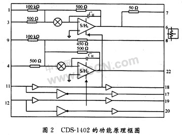
Under the general simple configuration, connect pin 7 and pin 8 to connect the output of S / H1 to the summary node of S / H2. When the CCD outputs the bias and video signals, pin 12 inputs a high level, causing S / H2 to enter the signal acquisition mode.
S / H2 uses the current-summary architecture, which subtracts the S / H1 output signal (offset signal) from the CCD output signal (offset plus video signal), leaving only the useful video signal. Pin 12 inputs a low level, causing S / H2 to enter the hold mode. After a transient stabilization process, useful video signals are output from pin 22. For the output signal of the CCD, the correlated double sampling circuit is the most commonly used processing method, mainly to remove the reset noise and kTC noise in the CCD signal. The processing effect is shown in Figure 3.
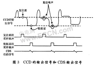
As can be seen from FIG. 3, when the pulse of the reset part is high level. The output signal of the CCD is sampled for the first time. The sampled signals are reset voltage, reset offset voltage and reset noise; when the pulse of the data part is high, the output signal of the CCD is sampled for the second time. The sampled signal includes reset voltage and reset. In addition to offset voltage and reset noise, it also includes useful video signals.
The signal sampled twice is output after passing through the differential amplifier circuit, which just removes the noise in the reset section. Because the noise of the two samples can be regarded as equivalent. Therefore, the reset noise can be basically removed by the correlated double sampling circuit.
4 Conclusion
Here, the noise of the CCD imaging device is analyzed. Starting from several noise sources (including transfer loss noise, reset noise, shot noise and dark current noise), the CDS related double sampling circuit is analyzed. Although it is limited to other reasons such as CCD noise and circuit process structure, the system has not reached the read noise level of the device itself, but the role of the CDS circuit is indeed obvious, and most of the noise has been eliminated. CDS technology has been widely used. CDS-1402 is a related double sampling circuit specially designed for CCD. Its sampling method is called "sampling-subtraction-sampling" technology, which is one sample less than the general CDS technology. This reduces the sampling spike.
LED flag screen totem on light poles or Outdoor Led screen kiosk, can save installation cost and time by pulling down and updating the printing advertising for light box. you can also unified management of intelligent management system. advertising can be really controlled,The Outdoor flat screen Is expected to become a large-scale media after as new carrier of advertising.
Small body, big world, It is not only small pixel pitch for Led Display, but a small era of Led screen!
The flag LED display kiosk on each road poles, not only can realize the comprehensive utilization of road poles, making the road no longer monotonous, but also can play content according to different festivals and beauty the city. At the same time, it will also provide the public with weather changes, environmental pollution and road access. bring more convenience to the public.
Priva provides professional intelligent Led light pole screen solutions and professional commercial LED display technology With a wealth of LED project engineering experience, Priva Led will meet customer`s varity needs.
Integrated design, easy to use
Operate controller inside, Optional of installation on back column and side of pole, Easy to transport & install.
Intelligent management and Large scale cluster control and management. easy and convenient
Managing multiple displays via cable, 3G, 4G, WAN and LAN; Could manage by mobile phone with APP. 1-1 and 1-N management One click to release, timing, updating AD.
Outdoor Led Flag Screen Totem,Outdoor Led Flag Screen,Outdoor Flag Screen,Slim Outdoor Led Poster
Shenzhen Priva Tech Co., Ltd. , https://www.privaled.com