Analysis of key technologies for interface design of automobile display
According to a survey by IMS Research, the number of car audio mainframes with video functions will increase from 8.5 million in 2006 to 26.6 million in 2015. In order to provide information to the driver without distracting his attention, the display needs to be installed away from the car audio host and project the screen to the back of the windshield. This video interface that combines image sources and panels is increasingly shifting from analog video technology to higher-quality RGB (red, green, and blue) digital video formats, which have become the standard interface used in LCD displays. The cable length for front-end display applications is usually kept in the range of 1 to 3 meters, while the cable for the rear seat entertainment (RSE) unit needs to be 8 meters or longer. This connection supports a gigabit / second data transfer rate, far exceeding the baud rate of traditional vehicle networks, and can be perfectly implemented using a point-to-point serializer / deserializer (SerDes) solution. Compared with the transmission of a wide parallel video bus, this chip set greatly reduces the number of transmission lines and connector pins, thereby achieving superior system-level advantages.
To meet the stringent requirements of automotive display interfaces, such as high data throughput, ultra-thin wiring, advanced signal conditioning, detectability, and ultra-low EMI (electromagnetic interference). National Semiconductor (NS) has developed the DS90UR905 / 6 and DS90UR907 / 8 SerDes chipsets. This product is an embedded XGA (1024 x 768) that can extend the resolution from QVGA (400 x 240) to 24-bit color depth Clock SerDes solution. The wide range of pixel clock frequencies allows car manufacturers to use a digital video display interface solution in their entire model series, which can cover from a small dual-screen dashboard panel, the LCD of the center console to a larger RSE display application.
Video application and SerDes concept
The target application area of ​​the SerDes component is the flat panel display link interface, which can connect the image host and the display through a long serial cable. Typical examples include: a central information display (CID), an instrument panel, an entertainment display on the headrest, or a roof-down display module for rear seat passengers, as shown in Figure 1. These new chipsets are part of the "FPD-Link II" series of products launched by NS. They can convert 27-bit digital RGB color information and time control signals of a video source into a single serial data with embedded clock information. The stream is transmitted on the twisted pair. The chipset uses high-speed differential signals on the I / O (input / output) layer, that is, while transmitting the actual signal on the "true" (positive) terminal, the corresponding signal is transmitted on the "complementary" (negative) terminal. Reverse polarity signal.
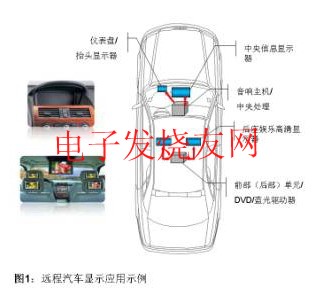
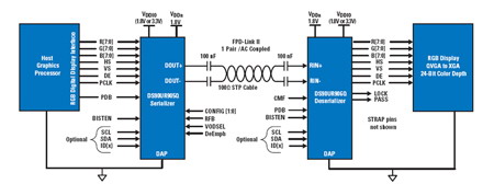
Figure 2 describes the concept of video transmission at the system level. In addition to the color and timing bits, there is an optional I2C control interface, which can replace the component configuration realized by the conventional pin with options. The chipset supports a color depth of 18bpp (bits per pixel) or 24bpp. A color display uses 3 sub-pixels (red, green, and blue) to define a single pixel. Since each pixel has 18 bits (6 bits red, 6 bits green and 6 bits blue), we can get 262,000 colors. Most human eyes can see more than 10 million colors, which explains why using 24bpp has become a trend: it can provide more than 16 million colors, which can achieve a richer user experience and smooth color gradients. The pixel clock range is now extremely wide: the frequency can be from 5MHz to 65MHz, which increases the serial link rate from 140Mbps to 1.82Gbps, covering all the mainstream resolutions of automotive displays.
Parallel LVCMOS input and output signals can be flexibly aligned with the rising or falling edge of the synchronous transmitter input and receiver recovery output clock (PCLK), this feature greatly simplifies the serializer to the image controller and the deserializer to Interface connection of LCD timing controller. Within a certain frequency band around the transmitter's parallel clock, the SerDes chipset does not require an external reference clock (quartz or oscillator) when "pre-synchronizing" the receiver's PLL. This synchronization can be guaranteed even during the transmission of all possible random data patterns. This is called the "random data lock" feature. This not only saves the cost of the reference component system, but also eliminates another potential source of electromagnetic interference. This feature also enables "hot swapping", that is, without any special ordering or training mode, you can perform assertion / de-assertion operations on the serial data stream sent to the deserializer.
Once the receiver PLL is locked at the frequency of the transmitter, this state can be displayed by the LOCK output flag pin to ensure the integrity of the data output by the receiver. The DS90UR907 / 8 chipset has all the features of the DS90UR905 / 6 chipset. The difference between the two ears is that the input and output are no longer parallel buses that send LVCMOS signals, but follow the open industry standard "FPD-Link". Many modern image controllers, display timing controllers, ASICs, and FPGAs support this "level one serialization" technology, which uses 3 data channels suitable for 18bpp or 4 data channels suitable for 24bpp, each of which There is a parallel clock channel. The transmission of electrical signals follows the open ANSI / TIA / EIA-644A standard, which is also known as "LVDS" (Low Voltage Differential Signal Transmission). The advantage of using this interface technology instead of conventional LVCMOS is that the use of differential signals can reduce electromagnetic interference and reduce the number of component pins, as shown in Figure 3.
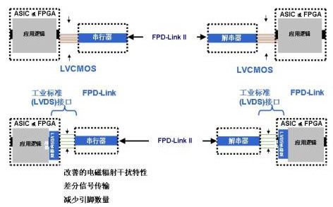
Figure 3 Advantages of FPD-Link system interface options
FPD-Link II payload
In each pixel clock cycle, 28 "sub-symbols" are time-division multiplexed on the differential I / O and converted into a serial data stream. The embedded payload contains 24 color bits, 3 timing signals (horizontal sync-HS, vertical sync-VS and data enable-DE) and additional bits. The interconnect line rate is 28x pixel clock. At 65MHz, this rate translates to 1.82Gbps. The serial data flow is limited by the "CLK1" HIGH bit at the front and the "CLK0" LOW bit at the end, thereby enabling a smooth transition between high and low levels between each frame, so that the serializer's PLL can synchronize with it And extract the embedded clock information. Two additional bits ("DCA" and "DCB" bits) are located in the middle of each frame, and they include timing signals embedded in the transition process of the DCA and DCB bits. In order to reduce the harmonic electromagnetic interference and improve the signal quality, the effective load bit has undergone randomization, balance and scrambling processing, and at the same time has established a DC balance for AC coupling.
Since the longer the cable connection, the more likely the ground potential drift between the transmitter and receiver modules. The AC coupling interface solution can achieve potential decoupling by using series capacitors in the transmission line. The DC-balanced encoder in the serializer and the DC-balanced decoder in the corresponding deserializer can achieve an even distribution between high and low bits on the serial link to prevent ISI (intersymbol interference) effects and capacitance Blocking in static mode. By configuring capacitors at both ends, this solution can also provide input / output short-circuit protection when the cable is damaged or there is a short circuit to ground or the net voltage on the board. Randomization and irregularity can not only ensure a good eye opening, but also minimize the electromagnetic interference of interconnected lines. Overall, the coding efficiency is higher than 85%.
Enhanced signal conditioning capabilities
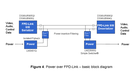
Signal conditioning technology plays a vital role in promoting long-distance high-speed connections. The signal recovery feature is used on the serializer side. Figure 4 is an example of a signal recovery operation. This series of converted bit streams are 0, 1, 000, and 1 in sequence. The single-ended (SE) waveform is given at the top of the graph, which can be measured relative to ground potential at the true value and output terminal. The bottom part of the graph shows the differential (DIFF) signal, which is equivalent to the differential voltage swing at the input of the receiver within its terminal range. For the first conversion, the first signal sent is 0, forming a fully differential swing. The next conversion is a 1, which is also the full voltage swing. Next in the C, D, and E time frames is a series of zeros, where the first zero is the full voltage swing. With the arrival of the second and third zeros in time slots D and E, the amplitude will decrease, indicating that it has been "restored" by the signal. Therefore, the static charge in the cable will be limited, otherwise it will increase with time. This causes the last bit 1 sent in time slot F to form a fully differential swing again. The signal restoration characteristic is usually to balance the internal energy of high and low frequency signals in the transmission line. The overall effect is a clear signal eye opening, followed by a single bit conversion after a long sequence of 1s or 0s. The signal restoration layer is programmable to adjust to the best compensation level for specific cable media.
In addition, the signal restoration feature has a good effect on the adjustable differential output voltage (Vod), that is, it can double the differential output voltage (Vod) transmitted by long cables. Signal restoration can restore the signal without significantly reducing the amplitude of the signal input by the receiver. The input terminal of the deserializer integrates a cable equalizer. When regenerating the entire signal waveform, this function is equivalent to a high-pass filter relative to the input signal, which can partially eliminate the low-pass filter effect caused by the transmission medium. The equalizer is programmable from 1.5dB to 12dB of gain. Of course, all the enhanced signal processing features can also be used in coordination to establish sufficient eye opening for error-free data recovery in long cable transmissions.
Spread spectrum clock
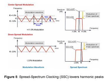
The deserializer is enhanced by an integrated configurable spread-spectrum clock (SSC) generator. At the receiver output bus, this will cause the output clock frequency and data spectrum to change slightly over time with a low modulation rate of tens of KHz. As shown in FIG. 5, the frequency change can occur near the center frequency of the nominal pixel clock ("center spread spectrum modulation"), or toward a lower frequency ("down spread spectrum modulation"). The spectrum spread percentage can be as high as ± 2%. Spread-spectrum clocks disperse the peak energy in a wider frequency range, which greatly reduces the level of electromagnetic interference noise, instead of converting all outputs at a constant frequency at a constant time point. The radiated noise at this time is concentrated in a narrow frequency band Inside, all output data is synchronized with the output clock, which allows the data and clock to be effectively expanded. In particular, the DS90UR906 receiver output has a low voltage (LV) CMOS interface option, which can greatly reduce electromagnetic radiation.
Enhanced diagnostic capabilities
Another feature is the built-in self-test (BIST) function. In this mode, the transmitter sends a pseudo-random code sequence (PRBS). The same sequence is generated internally in the receiver and compared with the received bit pattern. In order to find the best compromise between the overall test time and the lowest bit error rate that needs to be verified, the user can control the duration of BIST. When a payload with an error code is encountered, the PASS pin will be switched in a clocked manner. The PASS pin stores the final result of BERT (Bit Error Rate Test). If the test fails, it indicates that one or more load errors have occurred; if the test passes, it means that there is no error in the propagation and reception of the PRBS sequence. At the far end of the link, BIST does not require any data generator, data logging, or measurement system. Auto manufacturers can use BIST mode to test the system and check link operation. It can also be used as a test bed in the system development stage, sending data to the entire link without a video source, while only applying a clock signal to the transmitter. During the service or troubleshooting phase, system tests can be used to verify that the link is working properly, thereby locking the problem area on the host or display. Finally, when the car is started, the display interface can be routinely checked and verified for connectivity.
More enhancements
More enhancements include integrated termination resistors, which reduce the complexity of circuit board design, resulting in lower cost and smaller board space. A terminal common mode filter pin is provided at the input of the deserializer. It is recommended that the user ground the common-mode pin through a capacitor to ensure stability and ensure that the frequency is filtered out of the common-mode voltage. This will reduce the level of electromagnetic radiation to the outside world and at the same time increase the resistance to external noise sources. The resistance of a digital video link to external interference is usually studied through a large current injection (BCI) test, and the inductance is used to modulate a side current of up to 300mA onto the cable shield. The I / O bank is powered by VDDIO, either 1.8V or 3.3V. Such flexibility can take advantage of low interface levels and provide compatibility with downstream devices.
In general, when components are operated at 1.8V, the level of electromagnetic interference also decreases. In the event of a power failure, the output voltage state of the deserializer can be set to tri-state (high resistance) or low resistance. The pixel clock (PCLK) state can also be set to tri-state or low impedance to choose to stop the internal oscillator. In the latter case, the clock output will always exist regardless of whether there is an input signal. When the interface is only connected to a short-distance light-load bus, the receiver drive strength (RDS) feature can minimize the current consumption of the output bus, slow the output edge conversion rate, and ultimately reduce electromagnetic interference. The chipset supports an ultra-wide temperature range of -40 ° C to + 105 ° C and can be applied to various automotive electronic systems in different working environments. These chipsets are packaged in LLP, take up very little space, and have passed RoHS certification and AEC-Q100 Grade 2 standard for comprehensive automotive application certification.
Summary of this article
The new DS90UR905 / 6 and DS90UR907 / 8 FPD-Link II chipsets have many system advantages and enhanced features. The parallel video bus is serialized into a single group via an embedded clock, which reduces system cost, eliminates clock / data skew problems, reduces noise, and extends the link to long cable distances. The chipset supports all common automotive LCD resolutions from QWVGA to 24-bit color depth XGA. In order to promote system design, certification and approval, designers can focus more on how to reduce EMI characteristics. This can reduce the cost of protection requirements as much as possible without sacrificing reliability. The diagnostic BIST mode is good for factory testing and practical application, and also beneficial for troubleshooting testing and diagnosis. As the third-generation chipset in the FPD-Link II series, its components are based on proven and trusted IP protocols and are backward compatible with previous generation chipsets. The FPD-Link II chipset series represents a solution that is optimized for the automotive industry and supports true plug and play, because it does not affect performance when used in conjunction with low-density lines, and has high bandwidth, low power consumption, low EMI, durability and Can achieve autonomous link synchronization.
The GFCI will not protect you from line contact hazards (i.e. a person holding two "hot" wires, a hot and a neutral wire in each hand, or contacting an overhead power line). However, it protects against the most common form of electrical shock hazard, the ground-fault. It also protects against fires, overheating, and destruction of wire insulation.
Ground Fault Circuit Interrupter UL
Ground Fault Circuit Interrupter UL,Auto-Monitoring Ground Fault Circuit Interrupters,Ground Fault Circuit Interrupter,Outlet Ground Fault Circuit Interrupter
Hoojet Electric Appliance Co.,Ltd , https://www.hoojetgfci.com