Application of BA012Fx power amplifier in data transmission of WCDMA data card
As the data transmission rate of cellular networks increases, the demand for data transmission by data cards and mobile phones is also increasing. As far as WCDMA mobile phone power amplifiers are concerned, since mobile phones are often used in urban areas with dense base stations, high efficiency work is required in the low and medium output power range; on the other hand, for data transmission, the increase in transmission volume leads to PA Work more in high output power mode. For data cards and mobile phones, high efficiency is more important for data cards. Therefore, in addition to providing power amplifiers for mobile phones, many power amplifier manufacturers will also specifically develop power amplifiers suitable for data cards or high-speed data transmission. Mitsubishi Electric has developed a high-efficiency power amplifier "BA012Fx" for data transmission, which has been released recently. This article mainly introduces the design concept and experimental results of the BA012Fx series.
New power amplifier for data card based on GaAs HBT process
GaAs HBT (GaAs Heterojunction Bipolar Transistor) amplifiers are widely used in the field of CDMA mobile phones. This is because HBT has a higher output power density than FET (field effect transistor), and HBT can be driven by a bias voltage. Therefore, HBT power amplifiers have been developed in the field of mobile phones for many years.
Mitsubishi Electric has specially developed BA012Fx series power amplifiers for data cards. The series has 5 frequency bands, namely Band1 (1920MHz ~ 1980MHz), Band2 (1850MHz ~ 1910MHz), Band3 (1710MHz ~ 1785MHz), Band5 (824MHz ~ 849MHz), Band8 (880MHz ~ 915MHz), suitable for WCDMA networks in Asia, North America, Europe and Japan.
Figure 1 shows the appearance of BA012Fx series power amplifier module, the size is 3mm * 3mm * 1mm. The maximum output power is 670mW (28.25dBm), and the power added efficiency (PAE) is 45%, which has the highest level of performance among similar power amplifier products. This series of amplifiers integrates (i) attenuator: used to change the gain of the power amplifier and reduce the signal-to-noise ratio at low input power; (ii) coupler: used to detect the output power. We have also added a phase control function in the attenuation circuit, which can effectively reduce the phase error when changing the gain.
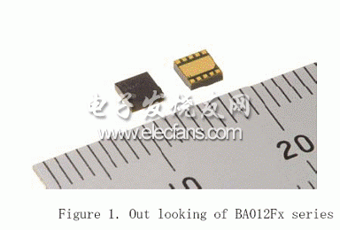
Figure 1 The external dimensions of BA012Fx series power amplifiers are only 3mm * 3mm * 1mm.
At present, mobile phone power amplifiers usually adopt the method of switching channels to improve performance at low and medium output power. However, the loss of the switching circuit that provides the path switching function will reduce the power added efficiency (PAE) of the entire power amplifier. Therefore, the BA012Fx series power amplifier does not use any switching circuit in the final output path, so as to achieve the purpose of high power additional efficiency at high output power.
Figure 2 is a block diagram of the data card amplifier. The power amplifier module consists of a two-stage amplifier and an attenuator located between the first-stage amplifier and the second-stage amplifier. Such a structure can reduce the noise figure in the low gain mode. The use of BiFET (Bipolar Field Effect Transistor) as an attenuator is to reduce the size of the chip because FET switching circuits can be provided on the same chip. Therefore, the chip size is smaller than the switch circuit using bipolar transistors. Three-dimensional electromagnetic analysis is adopted to make the circuit layout more reasonable. A single-step attenuation circuit is used, as shown in Figure 3. In the high-gain mode, SW1 of the FET is turned on and SW2 is turned off; the RF signal can be passed directly, and the loss is minimum. In the low gain mode, SW1 of the FET is turned off and SW2 is turned on, and the signal loses 14dB after passing through the series resistance and the parallel resistance. In order to compensate the phase change of the attenuator when switching, a series capacitor C1 is added.
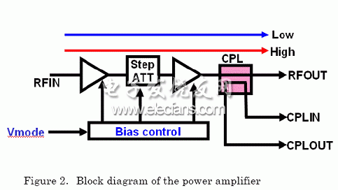
Figure 2: Block diagram of the power amplifier architecture.
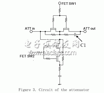
Figure 3: Attenuator circuit diagram.
This 4.7 inch inches LCD Writing Tablet is a mini size Electronic Writing Tablet , at the same time it can be used as a mobile phone shell, when you need do some record or draft, you can use LCD Writing Pad immediately. This Digital drawing tablet is a real good parter for business. An environment-friendly product, believe this Electronic Drawing tablet will bring you sustainnable and high-yielding.


4.7 Inches LCD Writing Tablet,Boogie Board Tablet,Boogie Board Writing Tablet,Boogie Board LCD Writing Tablet
Shenzhen New Wonderful Technology Co., Ltd. , https://www.sznewwonderful.com