Design principle of LM4702 high-fidelity power amplifier device
Design principle of LM4702 high-fidelity power amplifier device
The LM4702 is designed for consumer applications with high sound quality requirements and high power output. The output power of the amplifier can be adjusted according to changes in the supply voltage and the number of output devices. The audio amplifier designed with LM4702 can output more than 300W of power on each channel of 8Ω load. LM4702 pdf datasheet
LM4702 contains overheat protection circuit, it will stop working when the temperature exceeds 150 ℃. In addition, the LM4702 has a mute function, which will reduce the input drive signal and enable the amplifier output to become mute when enabled.
First, the functional characteristics LM4702 has 3 levels, across a wide range of applications and performance levels. LM4702C is aimed at high sound quality and high power applications; LM4702B (existing samples) can apply higher operating voltage; LM4702A (under test) is positioned as the highest-end application with the highest operating voltage. All three levels have ultra-wide operating voltages, including LM4702A ± 20 ~ ± 100V, LM4702B ± 20 ~ ± 100V, and LM4702C ± 20 ~ ± 75V. Its equivalent noise is 3uV, PSRR is 110dB, and THD is 0.001%. In addition, the LM4702 also has some excellent features, such as adjustable output power, few external components, external compensation, thermal protection and mute. They can be widely used in car audio, AV home theater, Hi-Fi audio, stage audio and industrial control.
Figure 1 shows the appearance and pins of the LM4702, and Figure 2 shows the typical application circuit of the LM4702. Figure 3 is a graph of THD + N and output power. 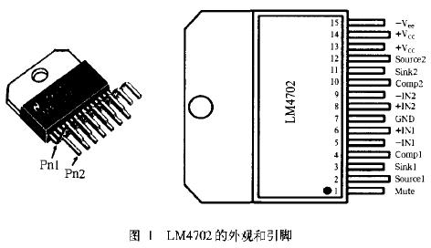
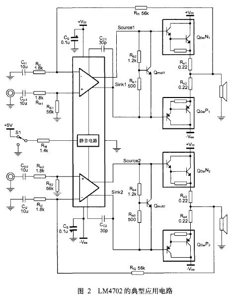
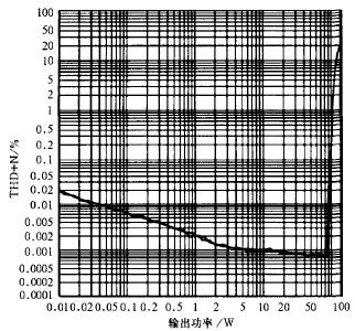
Figure 3 THD + N and output power diagram
(RL = 8Ω, VSupply = ± 50VDc)
1. Mute function The mute function of the LM4702 is controlled by the current flow into the mute pin. If the current flowing into the mute pin is less than 1mA, the chip is in mute state. This can be achieved by shorting to ground or floating the mute pin. If the current flowing into the mute pin is 1 ~ 2mA, the chip will be in playback mode. This can be achieved by connecting the power supply to the mute pin (Vmute) through a resistor (Rm). The current flowing into the mute pin can be determined by the formula
Imute = (Vmute-2.9) / Rm to calculate. For example, if a 5V power supply is connected to the mute pin through a 1.4kΩ resistor, the mute current will be .5mA, in the specified range. Vcc can also be used to power the mute pin, and Rm needs to be recalculated accordingly. It is currently not recommended to use a current flowing into the mute pin greater than 2mA, because the LM4702 may be damaged.
It is strongly recommended to quickly switch this function between mute and playback mode. It can be realized by toggle switch. One side of the toggle switch is connected to the mute pin, and the other side is connected to the ground or power supply through a resistor. Slowly increasing the mute current may cause a DC voltage to be generated on the output of the LM4702, causing damage to the speaker.
2. Thermal protection LM4702 has a complete thermal protection system to prevent the heat pressure caused by the system working for a long time. When the temperature inside the chip exceeds 150 ° C, the LM4702 automatically shuts down. When the temperature inside the chip drops to 145 ° C, it starts working again. If the temperature continues to rise to 150 ° C, the chip continues to shut down. Therefore, if a short-term failure occurs, the chip is allowed to heat up to a certain high temperature, but if it is a continuous failure, it may cause it to work in a 145 ℃ ~ 150 ℃ thermal switching conditions. In this way, the thermal stress of the chip is greatly reduced by cycling, which greatly improves the reliability under continuous failure. Because the wafer temperature is directly related to the temperature of the heat sink, the heat sink must be selected to ensure that the overheat switch does not trigger under normal conditions. If you use the best heat sink allowed by cost and space, you can ensure that any semiconductor device works stably for a long time.
3. Power consumption and heat dissipation In the playback mode, its operating current is constant, regardless of the input signal amplitude. Therefore, the power consumption is fixed for a given voltage, which can be expressed by the formula PDMAX = Icc × (Vcc-Vee). A quick calculation method for PDMAX is: when the current is about 25mA, it can be multiplied by the entire voltage (the current will change slightly within the working range).
The selection of the heat sink of the high-power amplifier is entirely to keep the temperature of the wafer at a certain level, so as to ensure that the thermal protection system is not triggered at a certain level. The thermal resistance between wafer and outside air θJA (JuncTIon to Ambient) is related to the environment. It consists of 3 thermal resistances, namely θJC (wafer to package case), θCS (package case to heat sink), θSA (heat dissipation) Film to the environment). θJC is 0.8 ° C / W in LM4702. After using heat-resistant alloy, θCS is about 0.2 ℃ / W. Because heat flow (power consumption) is similar to current flow, thermal resistance is like resistance, and temperature drop is like voltage drop. The power consumption of the LM4702 can also be expressed as
PDMAX = (TJMAx-TAMB) / θJA
When TJMAx = 150 ℃, TAMB is the ambient temperature of the system, and the maximum thermal resistance of θJA = θJC + θCS + θSA heat sink θSA is θSA = [(TJMAX-TAMB) -PDMA × (θJC + θCS)] / PDMAX
Again, the value of θSA is related to the system designer ’s requirements for the amplifier. If the ambient temperature of the amplifier is higher than 25 ° C, the thermal resistance of the heat sink needs to be smaller under other conditions.
4. Appropriate selection of external devices In order to meet the design requirements of the application, appropriate selection of external devices should be made. Let's talk about the choice of peripheral device values ​​will affect the gain and low frequency response. The gain of each non-inverting amplifier is determined by resistors Rf and Ri, as shown in Figure 2. The gain of the amplifier can be expressed as
Av = 1 + Rf / Ri
In order to obtain the best signal-to-noise performance, lower resistance values ​​can be used. Ri usually adopts 1kΩ, and then determine the value of Rf according to the design magnification. For LM4702, the magnification must not be less than 26dB, if less than 26dB will be unstable. Ri and Ci are connected in series (as shown in Figure 2) to form a high-pass filter, and the low-frequency response is determined by these two components. This -3dB frequency point can be obtained by the following formula
fi = 1 / (2Ï€RiCi)
If an input coupling capacitor is used to block the DC from the input, there will be a high-pass filter (combination of CIN and RIN). When using input coupling capacitors, RIN must be used to set the DC bias point at the input of the amplifier. The -3dB frequency response produced by the combination of CIN and RIN can be expressed by the following formula
fIN = 1 / (2Ï€RINCIN)
When the input is left floating, a large change in the RIN value may be observed at the output. Decreasing the value of RIN or smooth input can make this change disappear. When RIN decreases, CIN should be increased accordingly to ensure that the frequency response of -3dB remains unchanged.
5. Avoid thermal runaway when used as a bipolar output. When using a bipolar transistor for the LM4702 as the output stage (as shown in Figure 2), designers must pay attention to the problem of thermal runaway. Thermal runaway is caused by temperature dependence on Vbe (intrinsic properties of transistors). When the temperature rises, Vbe drops. In fact, when the current flows through the bipolar transistor, the transistor is heated, but the Vbe is reduced, which in turn increases the current intensity, and begins to cycle the process. If the system is not properly designed, this positive feedback mechanism will destroy the bipolar transistor of the output stage. The first recommended method is to use a heat sink on the bipolar output transistor to avoid thermal runaway, which will lower the temperature of the transistor.
The second recommended method is to use an emitter negative feedback resistor (Emitter DegeneraTIonResistor, Re1, Re2, Re3, Re4 in Figure 2). When the current increases, the voltage of the negative feedback resistor of the emitter also increases, so that the voltage between the base and the emitter can be reduced. This mechanism can help limit current and neutralize thermal runaway.
The third recommended method is to use a "Vbe multiplier" to clamp the bipolar output stage, as shown in Figure 2. This Vbe multiplier includes a bipolar transistor (Qmult, shown in Figure 2) and two resistors, one from the base to the collector (Rb2 and Rb4 in Figure 2), and the other from the base to the emitter Pole (Rb1 and Rb3 in Figure 2). The voltage from the collector to the emitter (which is also the bias voltage of the output stage) Vbias = Vbe (1 + Rb2 / Rb1), which is why this cycle is called a Vbe multiplier. When the Vbe multiplier transistor Qmult is connected to the heat sink like a bipolar output transistor, its temperature will be synchronized with the temperature of the output transistor. Its Vbe is also temperature dependent, so when the output transistor heats it up, it will draw more current. This will limit the base current into the output transistor, thereby neutralizing thermal runaway.
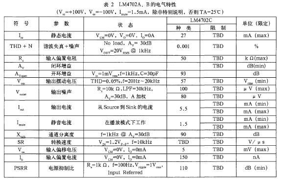
Table 1 shows the electrical characteristics of the LM4702 C operating voltage at ± 75V and ± 50V. Table 2 shows the electrical characteristics of the LM4702A and B operating voltage at ± 100V.
Table 1 Electrical characteristics of LM4702C
(Imute = 1.5mA, unless otherwise specified, TA = 25 ℃) 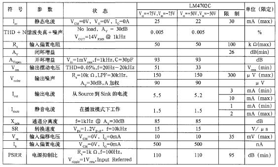
Note: 1. The typical value is measured at 25 ℃, which represents the standard of the parameter.
2. The test scope guarantees the average factory quality level of National Semiconductor Corporation.
3. The maximum / minimum specification range of the data is guaranteed by design, test and statistical analysis.
- Easy Installation
- Extended Life Up to 30,000 Hours
- High Shock & Vibration Resistance
- Humidity & Moisture Resistant
- No Buzzing
- No Mercury/Poisons
- Environmentally Friendly
- ETL/FCC Approved
- 1Year Warranty
-
Highly efficient, longer lasting LEDs will reduce your energy and maintenance costs.
LED Bulb With Remote Control,Smart LED Bulb With Remote Controller
Shenzhen Superlight Technology Co., Ltd. , https://www.superlighttech.com