Design of low phase noise local oscillator source for wideband CDMA transmitter
CDMA and CDMA are multiple access methods based on spread spectrum communication technology. It uses a unique code word to extend the message signal to a relatively wider frequency band, thereby reducing interference, enhancing the system's processing power, and distinguishing users. CDMA multiple access does not require split frequency and time, so the system capacity is higher. At present, the internationally mainstream third-generation mobile communication technologies (WCDMA, CDMA2000 and TD-SCDMA proposed by China) all use CDMA technology. CDMA transceiver will become the mainstream of future communication products.
As the heart of CDMA transmitter, the local oscillator has a decisive influence on the communication quality. CDMA technology has strict requirements on linearity and modulation accuracy. Therefore, according to the indicators of the whole machine (such as: error vector amplitude-EVM, adjacent channel power suppression ratio-ACPR), especially for multimode mobile phones that require high local oscillator sources To determine the specific indicators (phase noise, etc.) that can be achieved by the local oscillator source, and to design and optimize the circuit, has become a new challenge for designers of various CDMA communication equipment.
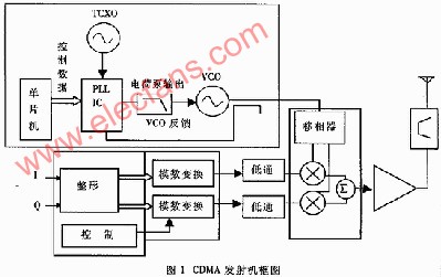
Figure 1 CDMA transmitter block diagram
This article introduces the design process of the local oscillator of a broadband CDMA transmitter, and provides a complete set of circuit indicators for CDMA transmitter local oscillator circuit (phase-locked loop), device selection and parameter setting, and the feasibility of the circuit design scheme. Sexual evaluation.
In addition, the EVM index of the transmitter system is simulated to obtain a reasonable phase error index of the local oscillator source. In order to facilitate the designer's optimization and simulation of the phase-locked loop, the author also wrote a set of ADS phase-locked loop simulation program, which is different from the common auxiliary program for optimization and calculation in the background. When using this simulation program, it is designed to adjust any parameter or device value and quickly obtain all the key indicators (such as: phase noise, spurs, stability) changes corresponding to the adjustment.
1 Introduction
The block diagram of the wideband CDMA transmitter is shown in Figure 1, where the upper left part is the local oscillator source circuit. The microcontroller controls the phase-locked loop chip (PLL IC) through the data section so that the circuit can be locked on different channels; the temperature-compensated crystal oscillator (TCXO) provides an accurate reference frequency source for the phase-locked loop; the voltage-controlled oscillator (VCO) The feedback signal and the frequency source are discriminated in the PLL IC. The phase discrimination output is output to the control terminal of the voltage controlled oscillator through the charge pump and the loop filter to control its output frequency.
2 Index setting
The main machine indicators related to the local vibration source are:
· Frequency stability: ± 2 × 10 -6;
· EVM: 15%;
· Bandwidth: 2.5MHz;
· ACPR: -40dB / ± 2.5MHz.
Based on the above indicators, the following specific indicators for the local oscillator source are obtained:
(1) Reference frequency source frequency stability: ± 1.7ppm (including temperature frequency stability, power supply voltage frequency stability, load traction frequency stability and annual aging rate accumulation).
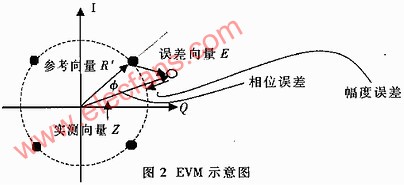
(2) Phase error: The phase error is determined by the error vector magnitude of the transmitter, or EVM (The error vector magnitude). EVM is often used to describe the modulation accuracy of the transmitted signal. Both TD-SCDMA and WCDMA standards use this standard to specify the quality of the transmitted signal. EVM is a measure of the difference between the ideal waveform and the actual waveform, as shown in Figure 2.
The measurement specifications provided by Agilent are widely used in measuring instruments and commercial simulation software. The specific internals are as follows:
Let Z (k) be the complex vector obtained by observing the transmitter under test through the ideal receiving filter at kT (T is the symbol period), and S (k) be the reference vector on the ideally normalized unit circle. Then Z (k) can be expressed as:
Z (k) = [C0 + C1 (S (k) + E (k))] Wk (1)
Where W = eΔr + jΔα is the frequency offset (Δα radian / symbol) and the rate of change of amplitude (Δr Neper (attenuation unit) / symbol); C0 is a constant complex offset, which represents the Unbalance; C1 is a complex constant representing the arbitrary phase and output power of the transmitter; E (k) represents the residual of the sample S (k).
Then the total square sum of error vectors is:
Among them, C0, C1 and W should make the above formula obtain the minimum value, under this condition, find the minimum error vector E (k) corresponding to each symbol.
EVM is defined as the root mean square value of the magnitude of the error vector E (k), namely:
Among them, N = MAX-MIN + 1, and MAX and MIN are the sorting numbers of the first symbol and the last symbol of the EVM measurement signal segment.
It can be seen from the above definition that the signal-to-noise ratio and nonlinearity of the transmitter may cause changes in EVM. And the influence of these factors on EVM can do simple linear superposition. In order to facilitate the determination of the specific indicators of the phase-locked loop through the EVM indicators, the author conducted a system simulation using ADS. In consideration of the nonlinearity of the power amplifier (PA)-the PA gain is set to 11.5dB, the third-order intermodulation point is 28.5dBm, the input power is 10dBm, and it is considered that the EVM of the local oscillator is set to <2% through simulation reasonable.
(3) Phase-detection frequency: Because the bandwidth is 2.5MHz, the phase-locked loop phase-detection frequency is also set to 2.5MHz.
(4) Spur phase noise (Spur): The spurious phase noise is generally determined by the ACPR (Adjacent Channel Power RaTIo), which is the adjacent channel power suppression ratio.
ACPR is sometimes called ACLR (Adjacent Channel Leakage RaTIo). It is defined as the ratio of the transmitted power to the measured power on the adjacent channel. Generally, it is mainly caused by the nonlinearity of the transmitter (particularly PA). But for the modulation method of direct up-conversion, the spur (Spur) of the local oscillator source on the adjacent channel also has a certain influence on the index.
To make Spur at this frequency point not affect the ACPR of the whole machine (ACPR <-40dBc / ± 2.5MHz), set the relative amplitude of phase noise at this point (± 2.5MHz) to -120dBc.
3 Device selection and parameter determination
3.1 Selection of reference frequency source
Through the determination of the above indicators, the frequency stability of the parameter frequency source should be: ± 1.7ppm (including temperature frequency stability, power supply voltage frequency stability, load traction frequency stability and annual aging rate accumulation). In order to facilitate the determination of the frequency division ratio of the phase-locked loop, set its operating frequency 20MHz = 8 × 2.5MHz (channel bandwidth).
3.2 Selection and parameter setting of PLL chip
a. Chip selection
In terms of chip selection, it was decided to use the National Semiconductor (NaTIonal Semiconductor) PLL chip. This design requires strict EVM modulation accuracy. The relationship between it and the phase noise of the local oscillator source is:
(4) In the formula, L (f) is the phase noise density. Therefore, the phase noise of the phase-locked loop becomes the key to the success of the design. First, choose the type of phase-locked loop (see Table 1).
Table 1 PLL IC types and performance comparison
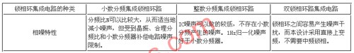
As can be seen from Table 1, a single phase-locked loop integer divider should be the first choice.
In order to achieve the purpose of minimizing phase noise, when choosing a phase-locked loop IC, the author focused on the 1Hz normalized phase detector noise index. Theoretically, this parameter is the phase noise caused by the phase detector when the phase frequency is 1 Hz. It is a technical indicator set based on the actual situation where the reference frequency source, frequency divider, and VCO's contribution to in-band noise is generally much smaller than the phase detector noise.
Phase noise = (1Hz normalized phase detector noise) + 10 · log (comparison frequency) + 20 · log (feedback branch frequency division ratio N)
Among all the single-loop frequency-divided PLL chips of NaTIonal Semiconductor, the 1Hz normalized phase detector noise value of the LMX2347 is the lowest, which is -220dBc / Hz, while other chips are generally above -210dBc. The computer simulation results show that when the noise value of the 1-Hz phase discriminator is -210dBc, the corresponding EVM value is 2.9%, and it is 1.06% at -220dBc (compared frequency is 2.5MHz). Therefore, the choice of LMX2347 becomes inevitable.
b. Determination of frequency division ratio
Since the channel width of this project is 2.5MHz, the ideal comparison frequency should be 2.5MHz. At this time, the frequency division ratio N is 1470 / 2.5 = 588, but the LMX2347 can only produce a continuous frequency division ratio in the range of 992 to 32767, so it is decided to choose the comparison frequency of 1.25MHz. The side effect of making this choice is that the overall phase noise increases by 3dB due to the increase in N value. Even if the phase noise characteristic of LMX2347 drops by 3dB, its overall characteristics are still at least better than other chips -210-(-220) -3dB = 7dB. And the actual simulation shows that when the comparison frequency is 1.25MHz, the EVM is 1.66%, which still meets the design requirements.
3.3 VCO selection and index setting
Phase noise is a key indicator of VCO design. According to formula (5), the phase noise of a reasonable VCO at 10kHz is -95dBc / Hz.
Among them, k is the lowest phase noise density in the phase noise spectrum, the unit is dBc / Hz, and p is the peak phase noise in the band.
To reduce the influence of the VCO input capacitance on the loop filter, the input capacitance should be less than 10pF.
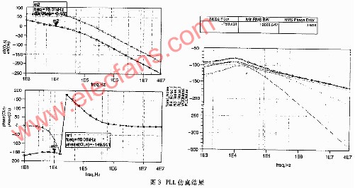
Figure 3 PLL simulation results
4 Circuit design and simulation
In order to facilitate the design and debugging of the circuit, the author has written a set of ADSPLL simulation programs. The program can flexibly select the filter order, and can give the phase noise, spur, phase margin and other parameters corresponding to the change after each parameter change, so that the designer can change the device value You can understand the overall characteristics of the PLL.
In the simulation software, Z21 in the Z parameter of the loop filter represents the loop gain, so that the loop filter topology can be adjusted at will. In addition, due to the advantages of the ADS software itself, the simulation software can optimize the parameters of any index to obtain the optimal circuit parameters. In terms of phase noise, the simulation program considers the phase noise of the 1Hz phase discriminator, the VCO phase noise, and the noise introduced by each resistance of the loop filter. The total noise is the superposition of various parts of noise at the output of the PLL, as shown in (6).
TotalNoise (f) = 10log (10PLLNoise (f) / 10 + 10CCONoise (f) / 10 + 10R2-Nsise (f) / 10 + 10R3_Noise (f) / 10 + 10R4_Noise (f) / 10 + 10TotolSpur (f) / 10 ) (6)
This program gives the open loop gain and phase change of the PLL circuit. The phase margin corresponds to the phase change when the gain is 0dB. Taking into account the influence of the local oscillator source on the ACPR parameters, the stray noise at the comparison frequency is added to the simulation program.
The spurious noise of PLL IC is composed of leakage spurious noise (Leakage Spur) and pulse spurious noise (Pulse Spur), and their calculation formulas are:
LeakageSpur = BaseLeakageSpur + 20log (LeakageCurrent / kφ) + SpurGain (7)
PulseSpur = BasePulseSpur + SpurGain + 40log (Fcomp / 1 · Hz) (8)
Among them, BaskLeakageSpur is a constant 16dBc, LMX2347 BasePulseSpur is -322dBc, SpurGain is the loop gain at the spurious frequency point, Leakage is the leakage current of the charge pump at the three-state high resistance, Kφ is the phase discrimination gain, Fspur is the stray The frequency of the frequency point.
In order to enhance the suppression of spurious noise to improve the performance of adjacent channel suppression (ACPR), and considering the comparison frequency of 1.25MHz, this design uses a 4th order loop filter. During the simulation process, the main goal is to suppress spurious noise. The optimized simulation results are shown in Figure 3. The line marked with "□" is the closed-loop gain and phase response, and the line marked with "×" is the open-loop response. The "○" line is the total phase noise.
(1) Phase noise parameters: According to the simulated phase noise density, the RMS Phase error = "0" .95 ° generated by the PLL circuit is obtained, and the EVM is 1.66% <2%, which meets the requirements of the index;
(2) Fixed time: 664.5μs;
(3) Stability: Phase margin 32 °;
(4) The sum of phase noise and spurious at 2.5MHz is -157.4. It can be seen that the spurious noise of this local oscillator source has very little effect on ACPR at 2.5MHz.
The above method can be widely applied to the design of various broadband CDMA (such as WCDMA, CDMA2000, etc.) communication circuits.
Jewish Candle is 3.8g Candle . Small Box Jewish Candle is high quality with strong box . it is very popular in Israel market . we usually called Multicolor Jewish Candle or 3.8G Jewish Candle . The Dia of Jewish Candle is 0.8cm , Length is 9.5cm .Box can do any colors or as your requirments . the noraml package is 44pcs/box 50boxes/ctn . it depends on you .
Fast shipment time, high quality product, and fast respond to any customer, we always online waiting your response. all the clients are our important person.
Jewish Candle
Jewish Candle,3.8G Jewish Candle,Small Box Jewish Candle,Multicolor Jewish Candle
Shijiazhuang Zhongya Candle Co,. Ltd. , https://www.zycandlefactory.com