FPGA Design and Implementation of Digital Correlator in Short Wave Spread Spectrum Communication System
Keywords: Digital Correlator FPGA, Hilbert Transform, StraTIx
Using FPGA devices can integrate the original circuit board-level products into chip-level products, which reduces power consumption and improves reliability. At the same time, it is easy to modify the design online. Circuit designers can implement specific digital signal processing algorithms in hardware through software programming, design input, simulation, testing, and verification. This method has the characteristics of versatility and can realize the parallel operation of the algorithm, so whether it is used as an independent digital signal processor or as a DSP chip coprocessor, it is currently a relatively active research field. 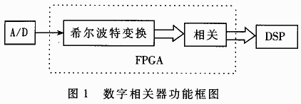
Shortwave communication has the characteristics of simple equipment, long communication distance, flexible maneuverability, low price and strong resistance to destruction, and has important application value. In the short-wave communication system, the receiver must perform a large number of multiply-add operations to perform related operations during signal detection and synchronization. In the case of high transmission rate and small sample interval, it is completely calculated by the central DSP processor of the system, and it is difficult to realize real-time processing. Using the characteristics of FPGA, it is a good solution to separate out the synchronous digital correlation part of the signal and design a dedicated digital correlator as the coprocessor of the central DSP processor to share this part of the work. This paper describes such a correlator based on FPGA design, which is used in the receiver of short-wave spread spectrum communication system to complete digital correlation functions.
1 Introduction to Stratix series chips
This article uses Stratix series chip to realize digital correlator. Stratix series is a new FPGA product launched by the well-known programmable logic device supplier Altera in 2002. Its main features are: the use of 1.5V core, 0.13μm all-copper process, the capacity is 10570 ~ 11140 logic units, embedding up to 10Mbit of three kinds of RAM blocks, namely 512bit capacity of small RAM, 4KB capacity standard RAM , 512KB of large-capacity RAM; with True-LVDS (tm) circuit, supports LVDS, LVPECL, PCML and HyperTransport (tm) differential I / O electrical standards, and has a high-speed communication interface; increased on-chip terminal matching resistance, improved Signal integrity simplifies PCB wiring; provides a complete clock management solution with a hierarchical structure and up to 12 phase-locked loops (PLL). 
The biggest feature of this series of chips is the programmable DSP module with embedded hardware multiplier and multiply-add structure, especially suitable for high-speed signal processing. This kind of DSP module is a high-performance embedded arithmetic unit, its running speed can reach 250MHz, and the data throughput performance of each DSP module can be as high as 2.0GMACs. It can be configured as a hardware multiplier, addition and subtraction device, accumulator and pipeline register, as shown in Table 1.
Table 1 Setting mode of single DSP unit
| Mode | 9bitx9bit | 18bitx18bit | 36bitx36bit |
| Single multiplier | 8 | 4 | 1 |
| Multiply accumulator | 2 (the result is 52bit) | 2 (result 52bit) | —— |
| Sum of 2 products | 4 | 2 | —— |
| Sum of 4 products | 2 | 1 | —— |
The Stratix series has up to 28 DSP modules, which can be configured as 224 (9bit & TImes; 9bit) embedded multipliers, which can provide flexible, efficient and valuable solutions for large data throughput applications. These DSP modules can implement a variety of typical DSP functions, such as finite impulse response (FIR) filtering, fast Fourier transform (FFT) functions, correlators, and encryption / decryption functions.
The Stratix series is supported by the new generation development software Qurtus II provided by Altera Corporation. This software strengthens the network function, the designer can obtain Altera's technical support directly through Internet. The MegaZard Plus_In Manager tool in Qurtus II software can easily customize some commonly used basic modules to meet different needs; designers can also make further improvements on the basis of customization and expand more functions .
2 FPGA design
The specific function of the digital correlator in the short-wave spread spectrum communication system is to receive the sampled signal after A / D sampling, perform the Hilbert transform on the sampled signal, and obtain another signal orthogonal to it; As the real and imaginary parts respectively, they perform correlation operations with the local sequence, and send the real and imaginary parts of the correlation values ​​to the DSP for subsequent processing, as shown in Figure 1. Only after the signal containing the correct sync header information is sampled and correlated with the local sequence, the modulo of the correlation value will have a peak; corresponding to the specific sync header frame structure of the origin, the correlation peak after correlation will also appear regular Sexual characteristics. In this way, the DSP can determine whether the signal is captured by first modulo the correlation value, and then judge and further process the information such as the interval, amplitude, and number of peaks where the modulus value appears. The following specifically introduces the FPGA design that completes the above-mentioned digital related functions. The internal structure block diagram of FPGA design is shown in Figure 2. 
2.1 Hilbert transform part
The RF signal received by the system is pre-processed by the front end and sent to A / D sampling, and then the sample values ​​are output to FPGA in a serial manner. Each sample value is expressed by the two's complement of 10 bits, which needs to be converted into a parallel signal with a width of 10 bits by a serial / parallel converter. The sample point value is to carry out the Hilbert transform first. There are many ways to implement the Hilbert transform. Here, a 129-order filter is used to implement the filter. The tap coefficients of the filter are generated by the MATLAB function remez, as shown in Figure 3. As shown.
The 10bit parallel signal is input to a 10bit & TImes; 129 RAM module. The cyclic writing method is used. The RAM module is similar to a barrel-shaped circular memory. The signal value stored in the RAM earlier will be overwritten by the new data. This is equivalent to the first-in first-out of the input signal shown in Figure 3. The tap coefficients generated by the MATLAB function remez are a set of decimal numbers with a large transformation range and decimal parts. In order to be able to perform subsequent hardware operations, this group of decimal numbers needs to be normalized and quantized, and they are mapped to a width of The range that can be expressed by the signed binary number of 14bit goes up, which is converted into the two's complement number of 14bit. This set of tap coefficients is fixed during the operation, so they can be solidified in the on-chip ROM module, read out synchronously with the value in the RAM, and then aligned by two sets of D flip-flops and sent to a 10 bit × 14bit signed multiplier accumulators do multiply-accumulate operations. The data width after multiplication is 24 bits, but when adding or subtracting signed binary numbers with a fixed data width, the result will exceed the range that can be represented by the fixed data width, that is, an overflow phenomenon, resulting in an incorrect calculation result, so It is necessary to reserve a certain amount of data width for the 129 accumulation operations performed here. Each time the product sign is extended by 4 bits and then the accumulation operation is performed, so that the output is a 28 bit signed number, which is the desired imaginary part. Since the tap coefficients are artificially enlarged many times in the normalized quantization process from decimal to binary, the real part corresponding to each imaginary part is output from the center tap after passing through a fixed multiplier , Expand the same multiple to keep the same with the imaginary part. 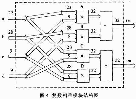
The multiply-accumulate module is the core unit of the Hilbert transform part. The unique embedded DSP module of Stratix device is used here. In Qawtus's Megawizard Plug_In Manager, select the Altmult_Accum (MAC) custom multiply-accumulate module. First, the system will prompt that only Stratix series can customize this type of module. The two input terminals selected in this example are 10-bit and 14-bit signed numbers, which are connected to the output terminals of RAM and ROM, and then the accumulated output terminal. Set to 28 bits. There are 4 bits intentionally reserved here to prevent data overflow during the 129 accumulations. After setting the clock, enabling, clearing, etc., the required multiply-accumulate module can be generated. During the compilation process, Quartus will automatically configure this part into the embedded DSP module without occupying the chip. Logical unit. In this way, the functions originally completed by several modules are realized by a single module, and the reliability of operation is also improved.
2.2 Related calculation part
The real part and the imaginary part of the sample value obtained by the Hilbert transform will be stored in two RAMs with 80 storage units, which are also written in a cyclic manner, similar to the barrel in DSP programming. Shaped storage area. Because the short-wave system used in this paper uses five sampling points per symbol, and the local sequence is a symbol corresponding to a value, so when doing correlation operations, from the current 80 sample values, every One value is taken from the four points, and a total of 16 sample values ​​are taken out, which are sequentially multiplied and accumulated with the 16 values ​​of the local sequence. In the next operation, the current sample point is shifted back by one bit, and the point calculation is performed in the same way. In this way, each sample value will produce a corresponding value corresponding to it. Reflected in FPGA, it requires RAM to start from the currently stored value and take one value every 4 units as output. In this way, within a sample interval, 16 values ​​are sequentially read from the RAM, and 16 local sequence values ​​synchronously read from the ROM are used to perform correlation operations. At this time, the multiplication in the correlation operation needs to be a multiplication of complex numbers, and the result is also a complex number. The real part and the imaginary part are output in two channels, and the two channels are accumulated separately to obtain the desired correlation value. Department and imaginary department. 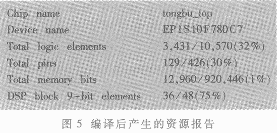
The complex multiplication module is an important link in the relevant calculation part. The signal value composed of the real part and the imaginary part read out from the RAM and the local sequence value read out from the ROM are subjected to complex multiplication operations here. The structure diagram of the complex multiplication module is shown in Figure 4. a, b, c, and d represent the real and imaginary parts of the signal and the local sequence, respectively, according to the formula (a + jb) × (c + jd) = (ac-bd) + j ( The combination of ad + bc) is multiplied, added and subtracted. What needs to be explained here is that the width of the data is limited to 32 bits considering that it will be connected to the DSP later. So for multipliers B and D, the result of multiplying 28 bits by 9 bits should be 37 bits. Here, when customizing the multiplier, it is forcibly limited to 32 bits, the excess sign bit of the highest bit is removed, and the lower 4 bits are discarded. The consequence of this treatment is to artificially reduce the product by 16 times. If the results of multipliers A and C are not processed and the addition and subtraction operations are performed directly, the results will cause serious errors. Therefore, for multipliers A and C, the output value should be artificially shifted to the right by 4 bits, similarly reduced by 16 times, and then the next addition and subtraction operations can effectively avoid the above errors. In this way, the four input values ​​are calculated after a few clock cycles, and the two output values ​​are the result of the complex multiplication. The four signed number multipliers here will be automatically configured to the embedded DSP module of Stratix device at compile time.
2.3 Overall control module and interface part
2.3.1 Overall control module
After the system is powered on, each module in FPGA is in the running state, and each module is connected to each other, and each has its own operation sequence. Therefore, in order to ensure that each module operates in sequence and obtains the correct result, a command and control module is required to perform Accurate control. Two master-slave counters working at 80MHz and 40MHz clocks are used here to control the modules in the relevant part and the Hilbert transform part. In a sample point interval, according to the different count values ​​of the counter, different combinational logic circuits are used to generate the enable and clear signals of each module to ensure that each module operates at the correct timing. In order to improve the efficiency of FPGA processing, the Hilbert transform part and related parts actually work in parallel. In the same sample interval time, the Hilbert transform part processes the currently input sample point data, while the related part is the result of the Hilbert transform part output in the processing of the previous sample point interval. The reason why the two parts can coordinate with each other and run in parallel is because there is various control information from the overall control module. 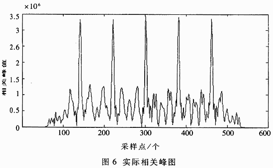
2.3.2 Interface section
FPGA has two interfaces, one with A / D interface and the other with DSP interface. In the interface part with A / D, there are three input terminals data_in, FS and SLCK, data_in is used to serially input the sample value converted from A / D; FS is a frame synchronization signal, which is used after input to FPGA Drives the overall control module inside FPGA; SCLK is the shift clock, which controls the shift of the serial transmission of data between A / D and FPGA. In the interface part with DSP, data_out [15. . 0] It is used to output the result of FPGA operation, and is connected with the data bus of DSP. A three-state gate is set inside FPGA, and the gate opening signal is the chip selection signal CE of FPGA. When the CE is not gated, the tri-state gate output is in a high-impedance state and does not affect the data bus of the DSP. During the time between each sample point, FPGA calculates the real and imaginary parts of the relevant values, latches them in four 16-bit latches, and sets the data_readey signal connected to the DSP high, indicating data already prepared. When DSP detects that data_ready is high, it will perform a read operation, use the upper bits of the address bus to generate a chip select signal to gate the FPGA, and select one of the four latches through the lower two bits of the address bus, A0 and A1. Read the upper 16 bits and lower 16 bits of the two 32-bit real and imaginary parts in sequence. FPGA internally counts the read operations of the DSP. After confirming that the data has been read out four times, the data_ready is set low until the next calculation is completed and then raised.
3 Simulation and verification
After each sub-module is designed, you can connect each module in graphical or text mode to compile the top-level design. The one with the smallest capacity in Stratix series is selected here: EP1S10F780C7. The compilation report generated after compilation is shown in Figure 5.
Whether it is an on-chip logic unit, on-chip RAM or DSP embedded block, the selected EP1S10F78080C7 chip still has a considerable amount of margin. However, if other series of chips are selected and there is no embedded DSP module, the on-chip logic unit occupied by it will be far more than that. 
After the compilation is complete, simulation and verification can be performed. This part can be divided into three processes. For the same piece of data, the simulation is first performed under Qurtus to produce a series of related values. Then, using its convenient drawing features in the MATLAB environment, it compiles a program to process the data in accordance with the method of data processing by each module in FPGA, and draws the graph of the processing result, as shown in Figure 6. Theoretically, the processing result should be exactly the same as the Qurtus simulation result, and the actual comparison shows that the two are indeed the same. Finally, in MATLAB, a program is theoretically compiled using pure software, the data is processed, and the correlated peak diagram after processing is drawn, as shown in Figure 7.
It can be compared that the amplitude and relative position of the correlation peaks displayed by these two graphs are basically the same. This shows that the results of data processing with FPGA are consistent with the results of the theoretical method, which also verifies the correctness of the FPGA design. Because FPGA performs only the initial correlation, the correlation peak amplitude shown in Figure 7 is not large. After the data is sent to the DSP, it needs to be subjected to secondary correlation processing, and then used for signal acquisition and synchronization.
This paper describes the FPGA implementation of the digital correlator used for signal synchronous acquisition in the short-wave spread spectrum communication system, and introduces the selected Stratix series devices. At a sampling rate of 384kbps, a 40MHz clock is provided externally. This correlator has stable working performance, correct calculation results, and can work well with DSP to complete the Hilbert transformation and related processing of sample data.
Best Battery Pack,Dewalt Battery Pack,Plug In Battery Pack,Dash Cam Battery Pack
Zhejiang Xinghai Energy Technology Co.,Ltd , https://www.headwayli-battery.com