Application and hardware design of VoIP voice card in router
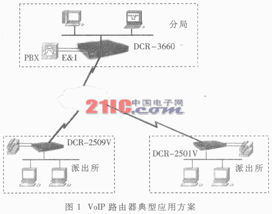
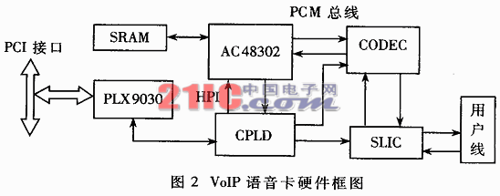
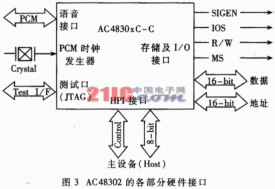
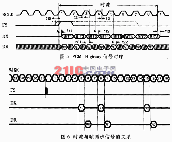
Abstract: This paper introduces the application of VoIP voice card in router, and describes in detail the hardware structure and working method of a voice card applied to router. Keywords: VoIP PCI FXS router voice compression 1 Application of VoIP in routers In recent years, VoIP (Voice Operater Internet Protocol) has brought a strong impact to the communications market. After the introduction of IP voice service, it has been widely welcomed because of its outstanding advantages over traditional telephones in terms of call costs. The application of VoIP technology in routers can greatly save the telephone expenses of enterprises or institutions with multiple departments operating in different places. Figure 1 shows the application of a VoIP router between a public security branch office and a police station. The routers DCR-2501V and DCR-2509V of the police station use FR (Frame Relay) or DDN lines to interconnect with the branch office's DCR-3660. The computers at each branch can be connected to the branch office's LAN or Internet through routers to achieve data communication; , DCR-2501V or DCR-2509V is connected to the ordinary telephone through the FXS voice port, and the branch office router is connected to the PBX through the E & M interface. This can not only realize data communication between various internal departments, but also make voice calls at zero cost. At present, the standards of VoIP mainly include H.H. recommended by the International Telecommunication Union Technology Department (ITU-T). The 323 system and the session initiation protocol (Session International Protocol, SIP) system recommended by the IETF. The former mainly implements multimedia service formulation on telecommunication networks, and the technology has matured. The latter is based on the dynamic Internet mode and is a simple signaling protocol for network conferences and phones based on softswitch technology. In China, the main choice is H. 323 technical standards to achieve VoIP, in H. Among the 323 series of standards, the audio compression coding standard is G. 711. G. 722, G. 723 and G729. This article will introduce the hardware design and working principle of a VoIP voice card that has been used in router products. The voice card is based on AudiCopus Company's VoPP (Voice Over Pack Prosecure, that is, voice packet processor) AC48302 design, adopts a PCI interface interface, can provide two FXS (Foreign Excel voice), and can be used in a flexible voice / status interface. In the series of routers developed by the company, the VoIP function is realized. The block diagram of its hardware structure is shown in Figure 2. The principle and role of each part of the hardware are introduced below. 2.1 PCI interface The router mainboard and the voice card are connected by a PCI bus, which is convenient for general use. The PCI interface chip PLX9030 is adopted to realize the conversion between the voice card local bus (HPI) and the PCI bus. Because the data traffic on the voice card is not large, there is no need to actively use the DMA method to transfer data to the memory space on the router motherboard. Therefore, the voice card works in the slave mode of the PCI. The AC 48302 receives or sends voice data through the interrupt mode. The data width and speed of the PCI bus are 32 bits / 33MHz. 2.2 CPLD part AC48302 adopts 8-bit parallel main processor interface HPI to exchange data with external CPU (ie router CPU). In this design, the timing of the HPI interface and the local bus interface of the PLX9030 is slightly different, and is adjusted through the CPLD. In addition, the router CPU can also control the CODEC and SLIC chips through the CPLD. AC48302 is a low-power, low-cost dual-channel voice packet processor launched by AudiCodes. It integrates a DSP core. The main characteristics of the chip are as follows: Support two channels of voice compression coding, voice compression standards include G. 729A, G. 723.1, G. 727, G. 726, G. 711. · T compatible. 38 or FRF. 11 fax relay (2.4 ~ 14.4kbps). · Call ID generation and detection, call progress and user-defined voice detection and generation. · Compatible with G. 168 echo cancellation at 25ms. · High performance effective voice detection (VAD) and comfort noise generation (CNG). · DTMF detection and generation. · A-law / μ-law optional Cord interface, with input and output gain control. · PCM Highway interface. · Parallel host processor interface (HPI). The hardware interface of each part of AC48302 is shown in Figure 3. The voice interface provides input and output channels for uncompressed voice and fax data. The voice interface provides four signal lines to form a PCM bus, which is directly connected to the PCM Highway of the external CODEC chip. The four signal lines are PCMIN, PCMOUT, PCMCK, and PCMFS. PCMIN inputs the PCM signal sent from CODEC. The DSP inside AC48302 is compressed according to the corresponding standard (such as G.729) and then handed over from the HPI port to the router CPU for forwarding. The PCMOUT is the opposite. The AC48302 decompresses the voice data sent from the router CPU according to a suitable standard, and then sends it to the external CODEC from the PCMOT port. After the digital / analog conversion, the CODEC returns to a voice signal. It is sent to the user terminal through the user interface. PCMLK provides a bit synchronization clock of 2.048MHz, while PCMFS provides a frame synchronization clock of 8kHz. 2.3.2 HPI interface In this design, the router CPU communicates with the AC48302 through the HPI port. The router CPU and DSP implement data exchange through the dual-port memory shared on the chip of AC48302. The mapping relationship of on-chip shared memory is shown in Figure 4. The HPI interface includes an 8-bit data bus and several control buses. The router CPU controls the AC48302 and accesses the on-chip storage space through three registers (HPIC, HPIA, and HPID). HPIC is a control register, used to select the high and low byte order of AC48302, generate and receive interrupts. HPIA is an address register used to address the 2K memory space on-chip. HPID is a data register, used to cache two bytes of data read and written at a time. The external CPU can access the HPID in a single word or block data mode. When accessed in block data mode, the HPIA register is automatically accumulated, which can reduce external CPU writes. The overhead of the HPIA register. The internal registers and memory of the AC48302 are 16 bits wide, so each time the external CPU accesses the AC48302 must use two bytes as the basic unit, the signal line HI / LO is used to select the high and low bytes, and the signals HRS1 and HRS0 indicate which is currently being accessed. register. In addition to the above two important interfaces, AC48302 also contains a PCM clock generator, a JTAG interface for testing, and a Memory & I / O interface for accessing external SRAM and processing channel auxiliary signaling. 2.4 CODEC interface chip The CODEC chip is responsible for decoding the PCM data sent after decompressing the DSP, and sending the filtered analog voice signal to the subscriber line interface chip SLIC. The SLIC converts it to 2-4 lines and sends it to the client; at the same time, CODEC It is also responsible for the PCM coding of the analog voice signal sent by SLIC, and then sent to the DSP chip for compression processing. In this design, the CODEC chip uses IDT's 4-channel PCM codec chip IDT821034. The chip has programmable gain settings, optional main clock (2.048MHz, 4.096MHz and 8.192MHz), up to 128 programmable time slots, optional A-law / μ-law, built-in digital filter, serial Line control interface, low power consumption and other characteristics. The main clock used in this design is 2.048MHz (E1 frame mode), which can be divided into 32 equal time slots (Slot0 ~ Slot31), and the reception and transmission time slots of the four channels can be controlled by writing to the serial control port Word for dynamic selection. The position of each time slot is referenced to the frame synchronization clock signal of 8 kHz. In the IDT 821034, the position of time slot 0 relative to the frame synchronization pulse has a delay mode and a non-delay mode (Figure 6 shows the non-delay mode). The PCM master clock (BCLK), frame synchronization clock (FS), receive data (DR) and transmit data (DX) together form the PCM Highway signal, which is connected to the AC48302. BCLK and FS correspond to the PCCMCK and PCMFFS of AC48302, respectively. Both clock signals are generated by AC48302; DR and DX correspond to PCMOUT and PCMIN of AC48302 respectively. Figure 5 and Figure 6 show the relationship between the timing of the PCM Highway signal and the relationship between the time slot and the frame synchronization signal. In order to send and receive data correctly between the CODEC and the DSP chip, the CODEC chip is generally selected to send data DX on the rising edge of BCLK and sample data DR on the falling edge, while on the other end, the AC48302 samples PCMIN on the falling edge of the clock and sends PCMUT on the rising edge. 2.5 Subscriber Line Interface (SLIC) chip In order to enable the voice card to provide the FXS interface function in the design, Ericsson's new SLIC chip PBL8370 was used to connect the user interface. It can generate high-voltage ringing current signal and provide automatic battery feed switching inside the chip. It has the function of circulating current ringing and ground key detection and 2-4 line conversion function. The chip integrates many traditional ringing relays, ring current generators and other devices in one chip, saving printed board space and cost. The hardware driver mainly completes the following functions: (1) Initialize the PLX9030 chip, configure related registers, and select the local bus working mode. (2) Initialize the AC48302 chip and start the DSP core inside the AC48302 to a normal working state. The start-up procedure of AC48302 is divided into the following steps in order: nuclear code (Kernel) download; program code (Program) download; initialization mode; start-up operation. (3) Normal operation of driving voice card. Receive processing off-hook interruption, put the SLIC into the correct state; configure each channel of the CODEC chip to send and receive data slots and gain control of the CODEC chip; receive and process AC48302 data packet processing interruption, the AC48302 passes the interruption method after each voice packet is processed Inform the router CPU to read the current data in the buffer or write the next packet to the buffer. This article uses the FXS interface, as long as the circuit behind the CODEC is slightly modified to achieve the FXO or E & M interface function. At present, the voice card solution has been widely adopted in router products. |
Led Panel Light,Led Panel Lamp,Smart Led Panel Light,Led Ceiling Panel Light
Changxing Fanya Lighting Co.,Ltd , https://www.fyledlights.com