Design of pre-amplifier circuit for weak optical signal
introduction
Photoelectric detection technology is an emerging detection technology that combines optics and electronics [1]. It mainly uses electronic technology to detect optical signals and further transfer, store, control, calculate and display [2]. In principle, photodetection technology can detect all non-electrical quantities that can affect the amount of light and light. The optical system can convert the non-electricity information to be detected into an easily accepted optical information, and then convert the optical information into electric quantity by using the photodetector, and further enlarge and process the circuit to achieve the purpose of outputting the electric signal [3] ]. Then use electronics, information theory, computer and physics to analyze the causes and laws of noise generation, so as to improve the corresponding circuit and better study the characteristics and correlation of the weak useful signals submerged by noise, so as to understand the non-electricity. status. The purpose of weak signal detection is to extract useful signals from strong noise while improving the signal-to-noise ratio of the output signal of the detection system.
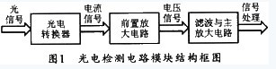
1 Basic structure of photoelectric detection circuit
The signals received by the photodetectors are generally very weak, and the signals output by the photodetectors are often buried deep in the noise. Therefore, in order to process such weak signals, it is generally necessary to perform pre-processing to Most of the noise is filtered out and the weak signal is amplified to the voltage amplitude required by the subsequent processor. In this way, it is necessary to output a signal to be detected whose amplitude is appropriate and which has filtered out most of the noise through the preamplifier circuit, the filter circuit, and the main amplifying circuit. The block diagram of its photoelectric detection module is shown in Figure 1.
2 Photodiode working mode and equivalent model
2.1 Photodiode working mode
Photodiodes typically operate in two modes: zero bias operation and reverse bias operation. Figure 2 shows the two modes of photodiode bias circuits. In the figure, in the photovoltaic mode, the photodiode can work very accurately linearly; in the lightguide mode, the photodiode can achieve a higher switching speed, but at a certain linearity. In fact, under reverse bias conditions, even if there is no light, there is still a small current (called dark current or no current 1). At zero bias, there is no dark current. At this time, the noise of the diode is basically The thermal noise of the shunt resistor; when back-biased, the shot noise generated by the conduction becomes an additional noise source. Therefore, in the process of designing the photodiode circuit, it is usually the most for one of the two modes of photovoltaic or light guide. Optimize the design, rather than optimizing both models [4].
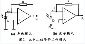
Generally speaking, in photoelectric precision measurement, the measured signals are relatively weak, so the influence of dark current is generally very obvious. In this design, since the signal to be detected is also a very weak signal, it is a primary task to avoid noise interference as much as possible. Therefore, the photovoltaic mode is adopted in the design.
2.2 Photoelectric diode equivalent circuit model
The working model of a photodiode operating in a photovoltaic mode is shown in Figure 3. It contains a current source that is excited by the radiated light, an ideal diode, junction capacitance, and parasitic series and parallel resistance. In the figure, IL is the leakage current of the diode; ISC is the current of the diode; RPD is the parasitic resistance; CPD is the parasitic capacitance of the photodiode; ePD is the noise source; Rs is the series resistance.
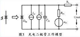
Since there is no voltage drop across the photodiode operating in this photovoltaic mode, it is zero biased. In this way, the key parasitic elements that affect circuit performance are CPD and RPD, which will affect the frequency stability and noise performance of the photodetection circuit. CPD is produced by the width of the depletion layer between the P-type and N-type materials of the photodiode. The narrower the depletion layer, the larger the value of the junction capacitance. Conversely, a wider depletion layer (such as a PIN photodiode) will exhibit a wider spectral response. Silicon diode junction capacitance ranges from approximately 20 or 25 pF to several thousand pF. The parasitic resistance RPD of a photodiode (also known as a "shunt" resistor or "dark" resistor) is related to the bias of the photodiode.
In contrast to the photovoltaic voltage mode, the photodiode in the light guide mode has a reverse bias voltage applied to both ends of the light sensing element. When this voltage is applied to the photodetecting device, the width of the depletion layer is increased, thereby greatly reducing the value of the parasitic capacitance CPD. The reduction in parasitic capacitance values ​​facilitates high speed operation, however, linearity and offset errors have not been optimized. The compromise design of this problem will increase the diode leakage current IL and linearity error.
3 circuit design
3.1 Main Amplifier Design
A lot of weak optical signals that need to be checked are usually non-electrical conversion through various sensors, so that the detection object is converted into electricity (current or voltage). Since the measured object itself is a weak amount and is limited by the sensitivity of various sensors, the obtained electric quantity is naturally a small signal and generally cannot be directly used for sampling processing. The photodiode preamplifier circuit in this design mainly functions as a current to voltage, but the subsequent circuit is generally an A/D conversion circuit, and the required voltage amplitude is generally 2 V. However, even then, the output voltage signal generally needs to continue to be amplified several hundred times, so the main amplification circuit needs to be applied. Its typical amplification circuit is shown in Figure 4.

The amplification factor of the main amplifier is A=l+R2/R3, where R2 is a feedback resistor. For the normal operation of the subsequent circuit, it is necessary to set reasonable R2 and R1 values ​​in order to obtain the output voltage of the desired amplitude. That is
3.2 filter design
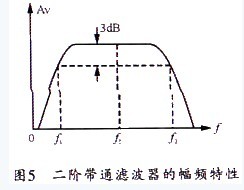
In order to make the circuit design simple and have a good signal-to-noise ratio, the signal is also processed by a band-pass filter. In order to ensure the accuracy of the measurement, the design adds a second-order band-pass filter circuit after the preamplifier circuit to remove noise outside the band of the wanted signal, including ambient noise and noise introduced by the preamplifier. The active bandpass filter used here can select signals in a certain frequency band and suppress signals outside the frequency band. The amplitude-frequency characteristics of this filter are shown in Figure 5. In Figure 5, f1 and f2 are the upper and lower limit cutoff frequencies, respectively, f0 is the center frequency, and the bandwidth is:
B=f2-f1=f0/Q
In the formula, Q is the quality factor, and the larger the Q value, the faster the gain decays as the frequency changes. This is because when the center frequency is constant, the Q value is larger, the narrower the frequency band passed, and the selectivity of the filter is good.
An active filter is a filter circuit that contains active devices such as semiconductor transistors and integrated operational amplifiers. Compared with passive filters, such filters are characterized by small size, light weight, low price, firm structure and integration. The operational amplifier has high input impedance, low output impedance, high open-loop gain and good stability, and is simple in structure and excellent in performance. This design uses a go-to-be amplifier for design.
This design uses a go-to-be amplifier for design.
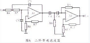
The second-order band-pass filter shown in Figure 6 is a second-order voltage-controlled voltage source (VCVS) band-pass filter whose filter circuit is implemented with an active filter and is low by a second-order voltage-controlled voltage source (VCVS). The pass filter and the second-order voltage-controlled voltage source high-pass filter are connected in series to form a band pass filter.
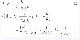
For the first part, the low-pass filter, the system requires a low-pass cutoff frequency of fc and its transfer function is:
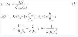
The second part is a high-pass filter. The high-pass cutoff frequency required by the system is fc. The transfer function is as follows:
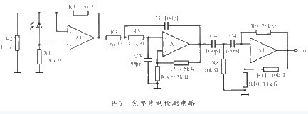
4 complete detection circuit design
The complete circuit designed by this photoelectric detection system is shown in Figure 7. For convenience of representation, R2 and R3 in the circuit are RT and RF in the previous equivalent circuit model. The pre-stage part consists of a photoelectric conversion diode and a preamplifier, which is also the core part of the photodetection circuit. The device uses a high-performance low-noise operational amplifier to achieve circuit matching and convert the photocurrent into a voltage signal to achieve several times of amplification. . However, although the preamplifier can be designed to be large, since the feedback resistor introduces thermal noise and limits the signal-to-noise ratio of the circuit, the pre-stage signal cannot be infinitely amplified.
5 Conclusion
This paper studies the principle and design method of photoelectric detection system. The parameters of the key components are determined by selecting and designing the relevant photoelectric conversion devices and preamplifiers from an economical and practical point of view. Proof of practical use: This design can meet the needs of general photoelectric detection occasions.
Headlight is Powerful light at the front of a vehicle. One motorcycle usually needs a one or two bulbs. It is depend on the original lamp design. Driver need power light to illuminate the road in front of them to keep them safe, so the halogen bulbs are usually been used as headlight. Halogen bulb can generate more light and has better working life hours. The supply voltage of halogen lamp is usually divided into 6V, 12V and 24V. The halogen lamp is made of tungsten, but it is enclosed in a smaller quartz glass shell. Normally, the halogen bulb will create ultraviolet when light, so we must use quartz coating to prevent head lamp been damaged by the ultraviolet generated by halogen bulb. To generate more light, the filament be heated to the very high temperature, so halogen bulb is hotter than a normal bulb.
Headlight Bulbs,LED Headlight Bulbs,Dual Color Yellow Lamp,Fog Light
Heshan Jianhao Lighting Industrial Co., Ltd. , https://www.sunclubtw.com