Absolute value circuit diagram
The figure below illustrates various types of absolute value circuits, which convert alternating current (AC) into direct current (DC). Starting with the most basic absolute value circuit shown in Figure (a), this circuit consists of a negative ideal diode circuit and an addition circuit, producing an output (U) equivalent to the absolute value of both half-cycles of the input voltage (Ui). When a capacitor (C1) is added to the inverting input and output of the operational amplifier (A2), the output becomes a smooth DC signal. The resistances should ideally satisfy R1=R2, R5=2R4, and Av=R6R5.
Moving on to Figure (b), it depicts a circuit with high input impedance. During the positive half-cycle, VD1 turns on, and A1 operates in a follower mode. In contrast, during the negative half-cycle, VD2 turns on. As shown in Figure (c), this is an absolute value circuit where all resistors are equal. In the positive half-cycle, U1 equals Ui, and VD2 does not conduct, leading to an output U equal to -(-Ui × (R5/R4)) or simply +Ui. During the negative half-cycle, VD1 remains off, and the output U2 is calculated as -Ui × [(R3+R4)/R2]. If all resistors are equal, U2 becomes -1/3Ui, resulting in an overall output U equal to -Ui(2/3+1/3) or simply -Ui.
Figure (d) displays an absolute value basic amplifying circuit using an ideal diode. Operational amplifiers A1 and A2 employ high-speed op amps such as LM318 and HA2525. Figure (e) presents an example of an absolute value high-speed amplifying circuit. Here, a constant current source formed by VT and VT2 biases A1 via voltage drops on RB1 and RB2. This configuration ensures simplicity while achieving a frequency characteristic for the absolute value amplifier of several hundred kilohertz or more.
Figure (f) showcases an absolute value circuit comprising an analog switch and a zero-crossing comparator. When the analog switch DG201 is activated during the positive half-cycle, A2 operates in a follower mode and outputs a high level. Conversely, during the negative half-cycle, A2 enters an inverter operating state, outputting a low level. The response characteristics of A2 and DG201 determine the highest operating frequencies, ranging from low frequencies up to 10 kHz.
As depicted in Figure (g), this standard DC conversion circuit transforms an input AC power of 1V to 10V DC using an ideal diode. Both input and output signals are linear, and the signal range is extensive. The potentiometer RP adjusts the gain, while C1 serves as the smoothing capacitor. Figure (h) represents another standard DC conversion circuit, but the rectification method differs. It employs two smoothing capacitors, C1 and C2.
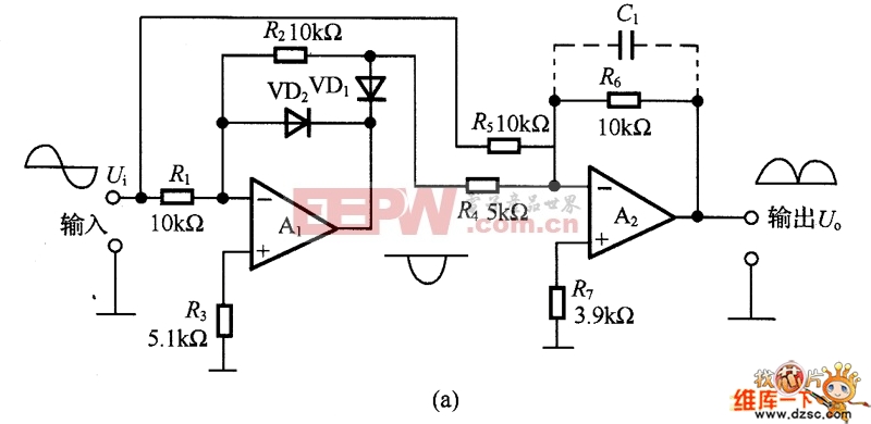 (a) The most basic absolute value circuit
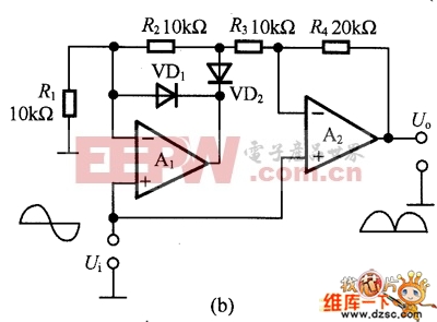 (b) High input impedance circuit
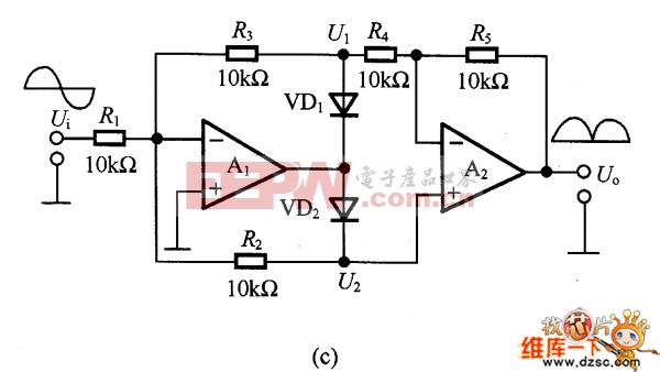 (c) Absolute value circuits with equal resistance
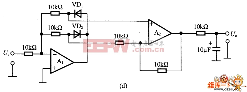 (d) Absolute value basic amplifying circuit using ideal diode
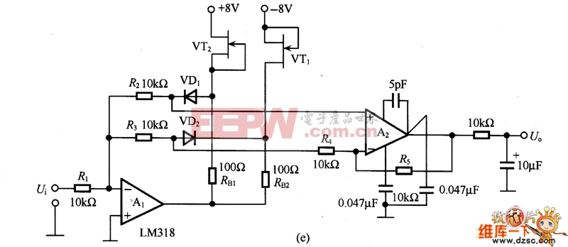 (e) Absolute value high speed amplifier circuit
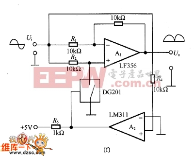 (f) Absolute value circuit composed of analog switch and zero-crossing comparator
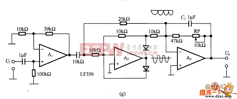 (g) One of the standard DC conversion circuits
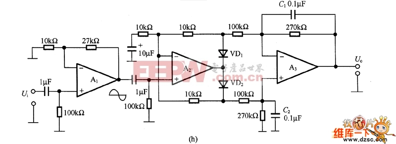 (h) The standard DC conversion circuit is shown as the absolute value circuit.
Digital Display Test Pen ,Power Tester Pen,Voltage Pen,Digital Voltage Tester
YINTE TOOLS (NINGBO) CO., LTD , https://www.yinte-tools.com