Design of Large Screen Display Control System Based on ARM+FPGA
0 Preface
With the development of computer and semiconductor technology, LED large-screen display system has become a display device integrating computer control, video, optoelectronics, microelectronics, communication and digital image processing technology. At present, LED large-screen displays are developing toward higher brightness, higher weather resistance, higher uniformity of illumination, greater screen, and higher reliability. The LED display industry is becoming an important part of China's electronic information industry. The development of large-screen display technology has greatly increased the amount of data that needs to be processed, the frequency of the system is getting higher and higher, the scale of the system is getting larger and larger, and the requirements for display control systems are constantly increasing. In the past, LED large-screen display systems were implemented with small and medium-sized integrated circuits, which were large in size, difficult to debug, and difficult to modify. With the further development of semiconductor technology and the wide application of large-scale integrated circuits, ARM has the characteristics of small size, low power consumption and strong data processing capability. PLD can meet the requirements of high-speed image data transmission speed of LED large-screen system and is flexible in design. . In view of this, the design uses ARM+RAM+FPGA solution to solve the problems of system running speed, addressing capability and power consumption, thus supporting stable display of larger visible areas and storing more display content.
1 system composition and principle
The system is mainly composed of a PC, a display control circuit and an LED display screen, as shown in FIG.
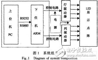
The PC is used as the upper computer in the control and is used for the control and management of the ARM of the latter stage. The upper computer is mainly used for human-computer interaction, completes the display data transmission to the display control circuit and sets the display effect of the LED display. The user transmits the edited text picture information and the corresponding control command to the control circuit part of the system through the serial communication on the host computer through the control software, and the LED display screen can cyclically display the edited text and pictures according to the mode selected by the user. The system also has an offline display function. After the user transmits the displayed content to the display control circuit portion, the upper computer can no longer participate in the display process, and the display system can display the information content to be displayed according to the mode set by the user. . The data conversion signal control part is implemented by ARM, and the scan driving circuit of the LED display screen is completed by using an FPGA. The communication between the upper computer and the lower computer adopts the standard RS232/RS485 computer data serial communication mode, which are relatively independent, but coordinate with each other. The display screen is made up of LEDs and is composed of LED dot matrix display units. The display of this design is 16 rows & TImes; 256 columns, using 640 & TImes; 480 dot matrix structure.
2 system hardware design
2.1 display control circuit
An important part of the display control circuit system is mainly composed of an input interface circuit, a data conversion and signal control circuit, and a scan drive circuit, as shown in FIG. 2 .
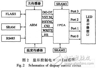
When the display is made bigger, that is, the more dots on the screen, the more data is sent to the display, the time for data transmission and control will increase, and the longer the time for completing one screen scan will be. Therefore, this factor must be considered in the design. The key to meeting this requirement is to increase the execution speed of the program, and you can choose a faster CPU or digital signal processing chip ARM. This design uses ARM-based 32-bit embedded RISC as the processor, S3C4510B is fully capable, the microprocessor has higher speed and larger storage capacity.
The upper computer sends the instruction set to the ARM microprocessor through the serial port through the RS232/RS485 converter. The ARM microprocessor stores the received instruction set in the external FLASH, and the content is not lost after the power is off, and the ARM external expansion is two. The chip SRAM is used to store fast-calculated data. The light sensor and temperature sensor are used to measure the light and temperature of the outside world, so as to change the brightness of the display with the intensity of the light, and display the external temperature on the display. The FPGA completes the scanning and driving process of the LED screen, and the internally solidified digital logic is responsible for generating the screen display control signals (serial shift clock, row latch signal, row selection signal, etc.), and two external SRAMs for external division are used for Read grayscale data. At the same time, the FPGA reads the gray data signal from the SRAM and converts it into the upper screen data and serially outputs it to the corresponding color signal data bus. The two external SRAMs of the FPGA form a data buffer and switch area. The ping-pong logic is used to write data to a piece of memory at a certain time, and the other piece is read by the FPGA logic and then sent to the display screen. The high-speed screen of the data and the continuity of the display. ARM external configuration of large-capacity SRAM and FLASH memory, compared with the traditional display control circuit, can support a larger display area, store more display content, get better display.
2.2 scan drive circuit design
The scan drive circuit portion of the LED display is implemented by an FPGA, as shown in FIG.
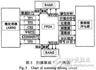
The scan driving circuit mainly performs functions of reading and transmitting gray scale data, generating grayscale data of the upper screen, generating a shift clock, controlling the luminance signal, generating four partition latch signals, and notifying the ARM to transmit data. These functions are all done in one FPGA, which reduces the size of the display control board, and since the FPGA function is implemented in the hardware description language VHDL, the VHDL language can be used to verify the feasibility and correctness of the system solution. Then, it is realized by FPGA hardware, which can greatly shorten the development cycle, make the design flexible and easy to modify. At the same time, FPGA has greatly improved circuit performance due to its high integration, high speed and high reliability, and short development cycle.
The implementation of this design requires FPGA to provide a large number of I / O pins, of which I / O pins include (1) system bus interface: 8 data bus, 5 control signal lines, 3 brightness signal lines, input line 1 Root, reset signal line 1 root, a total of 18; (2) dual-body SRAM bus interface: 15 address bus, 8 data bus, 2 read and write control signals, a total of 50; (3) display control signal output interface : 1 shift clock signal, 1 row latch signal, 4 rows; (4) Display pixel data output interface: 3 red, green and blue. A total of 18+50+6+3=77 I/O ports. In order to increase the size of the LED display by a factor of two, that is, the required number of I/O ports increases, and the number of macrocells required for the internal functional logic described in the VHDL language is used, 256 macrochips are required. The 32-bit PolarPro QLlP300 chip is used.
2.3 Static Memory SRAM Selection
The externally extended two-chip SRAM is required to meet the data reading speed of the upper screen. Considering the width and capacity of the stored data, this design uses the IS61C1024 chip of ISSI (Integrated Silicon SoluTIon Inc.). The chip has a storage capacity of 128 kB, an 8-bit data width, a maximum read/write speed of 25 ns, a power supply voltage of 5 V, a read/write frequency of up to 40 MHz, and high-speed asynchronous read and write operations without waiting time. To meet the storage requirements of one-screen text and image data information, two SRAMs use a two-body switching technique to complete the data storage and reading process.
Led Tube light
LED tube is commonly known as light tube, daylight tube, its light source using LED as the luminous body. Led tube has many advantages, using led as the light source, light efficiency is higher, more energy saving, longer service life, and more environmental protection. It is generally used for general lighting, office buildings, shopping malls, restaurants, schools, homes, factories and other Indoor Lighting. LED tube can save more than 70% electricity, and its life is more than 10 times that of ordinary light (in theory, it can reach more than 50,000 hours). It does not need to be replaced frequently. At the same time, LED tube has soft light, pure color, which is beneficial to people's vision protection and health.
LED Fluorescent Light,LED Fluorescent Tube,LED Fluorescent Replacement,LED Tube Light Fixture
JIANGMEN LEDERLIGHT LIGHTING Co.,LTD , https://www.lederlight.com