Design and Application of New RF Switching Circuit
Usually there are many input and output ports in the RF system, and it is expensive to analyze the scattering characteristics with a multi-port network analyzer. Therefore, it is generally necessary to switch the signals of multiple input and multiple output with a switch, and then perform analysis and measurement with a relatively simple two-port network analyzer. In the nuclear magnetic resonance system, the number of channels of the general receiving system is smaller than the number of antenna coils, so the multi-loop coils should also be switched to select and use.
In the current general design, the switching function is implemented by using a ready-made switch chip. However, most switch chips are not reliable, easy to damage, and the power supply lines are complicated. For example, although the SW-437 chip can perform a simple switching function, it has a very high antistatic requirement. The general laboratory and production workshop conditions are difficult to meet the requirements of the manufacturer, so the practical application is inconvenient and easy to damage. In this design, a new type of RF switch conversion circuit using pin diodes is designed. The function realized is to select any two RF signal outputs for the four RF input signals.
Overall structural designThe switch will be applied to this resonant test system, which is based on the LabView software platform and is provided by the computer to the voltage control signal. The control signal is a digital signal and can only provide high and low levels, the high voltage is 5V, and the low voltage is 0V, so voltage conversion is required to provide to the switching circuit. The whole circuit consists of two parts: a voltage conversion circuit and a radio frequency switching circuit. Eventually, when LabView supplies 5V, the voltage input to the switch is 10V and 0V; when LabView provides 0V, the voltage input to the switch is 0V and 10V.
Voltage conversion circuit design:
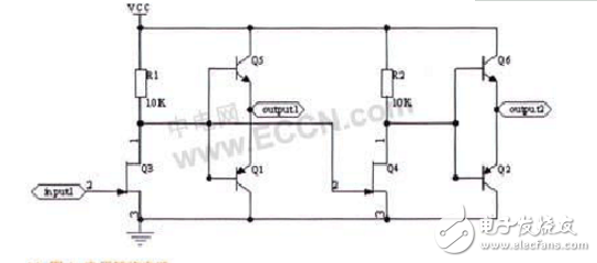
The voltage control signal provided by the computer to the RF switch based on the LabView platform is a digital signal, the extreme high level is 5V, the low level is 0V, and the voltage control signal required by the RF switch is 10V, so it is necessary to convert 5V to 10V, 1 is a conversion circuit diagram. When the input signal input1 is 5V, Q3 is turned on, Q5 is turned off, and Q1 is turned on, so output1 is 0V. At this time, Q4 is cut off, Q6 is turned on, Q2 is turned off, and output2 output VCC is 10V. Eventually, when LabView supplies 5V, the voltage input to the switch is 10V and 0V. When the input signal input1 is 0V, Q3 is turned off, Q5 is turned on, and Q1 is turned off, so output1 is 10V. At this time, Q4 is turned on, Q6 is turned off, Q2 is turned on, output2 output is 0V, and the voltage input to the switch is 0V and 10V. Meet the operating voltage of the microwave RF switch.
Switch circuit design:
Design idea: use DC signal to control the on and off of the pin diodes diode, input RF signal through the turned-on diode output; change the control logic to change the output of the control input RF signal.
The design steps are as follows:
1) Design DC control circuit
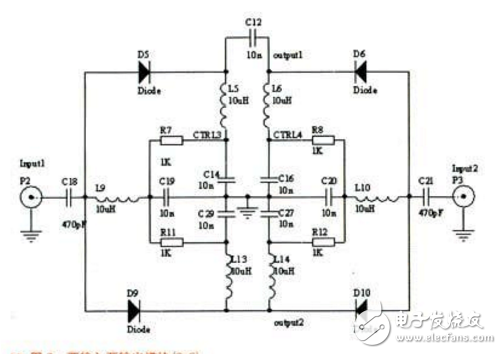
In this circuit, the diode is INFINEON technologies BA592, and the best performance current is 5mA. Therefore, to meet the requirements of the diode, the control voltage added in the design is 10V, and the loop resistances R7, R8, R11, and R12 are all 10K.
2) Design an AC signal circuit according to the requirements of scattering characteristics
Since the center frequency of the circuit operation is 63.6MHz, which belongs to the high frequency band, it is necessary to ensure the matching of the input and output ports. Specifically, when one RF signal is output, the other signal should be matched with 50R resistor. Since this circuit has both a DC signal and an AC signal, it is important to separate the two so that they do not affect each other. Apply a 10nF coupling capacitor according to the frequency requirement, short circuit to the AC signal, and open circuit for the DC signal; apply a coupling inductor of 18μH to open the AC signal and short circuit the DC signal.
3) Basic module and connection between modules
Figures 2 and 3 are basic modules. Figure 2 shows a two-input two-output module (2x2): a DC voltage of 10V is applied between CTRL3 and CTRL4, that is, when CTRL3 is applied with 10V and CTRL4 is applied with 0V, diodes D6 and D9 are turned on. At this time, the input signal input1 is output through the diode D9, and the input signal input2 is output through the diode D6. When the control signal is reversed, that is, CTRL4 adds 10V voltage, and CTRL3 adds 0V voltage, diodes D5 and D10 are turned on, input signal input1 is output through diode D5, and input signal input2 is output through diode D10. Thereby, two input signals are simultaneously outputted, and the purpose of the input signal output direction can be changed by the logic of the control signal.

3 is a two-input-output module (2x1): the control signals 7, 8 control the on and off of the diode, and the diodes D13 and D16 are simultaneously turned on or the diodes D14 and D15 are simultaneously turned on, which is the same as the module 1. However, the two input signals have only one output, and the other output is connected to the 50R resistor to achieve matching, thereby realizing two inputs and one output, and the function of selecting which output through the control signal can be realized.
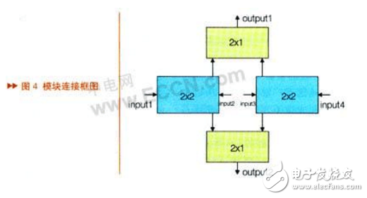
Figure 4 is a block diagram of the module connection of the entire circuit, clearly showing the logical relationship between the modules, and the signal transmission process. For example, when the control logic is 1111, the input signals input1 and input3 are input to the 2x1 output module through the diode from the upper path. Since the control logic is high, only input1 can be output from output1; and the input signals input2 and input4 are input from the lower path through the diode. The lower 2x1 output module, also because the control logic is high, only input2 can be output from output1, thus achieving four input signals, only input1 and input2 are output from output1 and output2 respectively. When the control logic is changed, the output of the desired input signal can be selected. For example, if the control logic is 1110, the output signals are input1 and input4. The 4-way control signal can control 12 states, correspondingly establish a database, and write the corresponding program to the test through LabView.
With the development of the times, the consumption level of people is gradually increasing. At the same time, people's entertainment methods are beginning to diversify, especially for modern young people. As a result, different kinds of electronic products are starting to be in people's lives, and the booming Electronic Cigarette industry reflects this.
Described including the upper shell, the upper shell at the top of the smoke outlet, as described in the bottom of the upper shell with airway, described with the smoke outlet in the airway and also to match the upper shell, the lower part of the shell described the airway in the direction of the lower shell extension, as described in the lower shell near one end of the upper shell is equipped with oil mouth, described the lower shell with batteries, described at the bottom of the bottom shell has come in The air port is provided with an oil storage bin in the lower shell, and the air passage passes through the oil storage bin and is provided with a heating atomization bin at one end away from the smoke outlet. The utility model has beneficial effects: it can meet the smoking habit of different users, avoid the premature end of the use experience caused by excessive consumption of smoke oil, and indirectly prolong the service time and life of the product.
Refillable E-Cig Oem,Refillable Vape Pod,Refillable Vape Pen Oem,Refillable Mod Oem
Shenzhen MASON VAP Technology Co., Ltd. , https://www.e-cigarettefactory.com