I will tell you the most complete chip packaging technology.
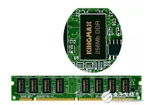
   Obtaining an IC chip goes through a long process from design to manufacturing. However, a chip is quite small and thin, and if it is not protected, it will be easily scratched and damaged. In addition, because the size of the chip is small, it would not be easy to manually place it on the board if a larger size housing is not used. At this time, packaging technology comes in handy. This article introduces 28 chip packaging technologies.
1. BGA|ball grid arraye
Also known as CPCC (globe top pad array carrier). One of the spherical contact display, surface mount packages. A spherical bump is formed on the back surface of the printed substrate in place of the lead, and the LSI chip is mounted on the front surface of the printed substrate, and then sealed by a molding resin or a potting method. Also known as a bump display carrier (PAC). The pin can exceed 200 and is a package for multi-pin LSI. The package body can also be made smaller than the QFP (four-sided pin flat package). For example, a 360-pin BGA with a 1.5mm center-to-center distance is only 31mm square; a 304-pin QFP with a 0.5mm center-to-center distance is 40mm square. And BGA doesn't have to worry about pin deformation like QFP.

The package was developed by Motorola, USA, and was first adopted in devices such as cellular phones, and then popularized in personal computers. Initially, the BGA has a pin (bump) center-to-center distance of 1.5mm and a pin count of 225. There are also some LSI manufacturers that are developing 500-pin BGAs. The problem with BGA is the visual inspection after reflow soldering. The US company Motorola called the package sealed with molded resin called MPAC, and the package sealed by the potting method is called GPAC.
2.C-(ceramic)
C-(ceramic) indicates the mark of the ceramic package. For example, CDIP stands for ceramic DIP. It is a mark that is often used in practice.

3.COB (chip on board)
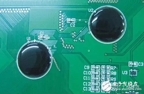
The chip-on-board package is one of the bare chip mounting technologies. The semiconductor chip is placed on the printed circuit board, and the electrical connection between the chip and the substrate is realized by a wire stitching method and covered with a resin to ensure reliability. Although COB is the simplest die-on-die technology, its packaging density is far less than that of TAB and flip chip bonding.

4.DIP (dual in-line package)
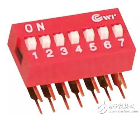
Dual in-line package. One of the plug-in packages, the leads are led out from both sides of the package, and the package materials are plastic and ceramic. European semiconductor manufacturers use DIL. DIP is the most popular plug-in package, and its application range includes standard logic IC, memory LSI, and microcomputer circuit. The pin center is 2.54mm apart and the number of pins is from 6 to 64. The package width is typically 15.2mm.

Some packages having a width of 7.52 mm and 10.16 mm are referred to as SK-DIP (skinny dual in-line package) and SL-DIP (slim dual in-line package) narrow body type DIP, respectively. However, in most cases, it is not differentiated and is simply referred to as DIP. In addition, ceramic DIP sealed with low melting point glass is also known as Cerdip (4.2).
4.1 DIC (dual in-line ceramic package)
Another name for DIP (with glass seal) in ceramic package.
4.2 Cerdip
Glass-sealed ceramic dual in-line package for circuits such as ECL RAM, DSP (Digital Signal Processor). Cerdip with glass window is used for UV-erasing EPROM and internal microcomputer circuit with EPROM. The center of the pin is 2.54mm and the number of pins is from 8 to 42. In Japan, this package is denoted as DIP-G (G is the meaning of a glass seal).
4.3 SDIP (shrink dual in-line package)
Shrinkage type DIP. One of the cartridge type packages has the same shape as the DIP, but the lead center distance (1.778mm) is less than DIP (2.54mm). Therefore, this is called. The number of pins is from 14 to 90, and there are two kinds of ceramics and plastics, also known as SH-DIP (shrink dual in-line package).
It can prevent scratches and dirty fingers, and the transparent design can clearly display the screen content. The Screen Protector is easy to use and has no bubbles to maintain touch sensitivity.
The Soft Protective Film can accurately adapt to all curved screens of the Samsung series.
With a self-healing design, it can protect the display of the device from damage without leaving bubbles and maintain the sensitivity of the touch screen.
The oleophobic and waterproof coating helps minimize oil stains and fingerprints on the display.
If you want to know more about Screen Protector For Samsung products, please click the product details to view the parameters, models, pictures, prices and other information about Screen Protector For Samsung.
Whether you are a group or an individual, we will try our best to provide you with accurate and comprehensive information about the Screen Protector For Samsung!
Screen Protector For Samsung, Hydrogel Curved Screen Protector, TPU Film, Anti-Scratch Screen Protector,Curved Screen Protective Film
Shenzhen Jianjiantong Technology Co., Ltd. , https://www.tpuprotector.com