Realization of Digital Frequency Agile Combiner with Low Phase Noise and High Purity Spectrum
Abstract: The design of an X-band frequency synthesizer, and this program will direct digital lock combination, rapid completion agility feature.
introduction
Modern radars place higher and higher requirements on frequency synthesizer phase noise, fast agility, flexible waveform generation, and in-band spurs. The full coherent direct frequency synthesizer has high frequency stability and short frequency hopping time. The shortcoming of the direct frequency synthesizer is spurious suppression, and the amount of equipment is huge. The disadvantage of the phase-locked frequency synthesizer is that if the total frequency division ratio of the loop is too large, the phase noise of the output will be seriously deteriorated; and the frequency conversion speed is relatively slow. Therefore, the direct frequency multiplication and digital lock are combined, and the fast switching speed of the switch, the frequency stability of direct frequency multiplication, and the flexibility of digital phase lock are used to complete the design of the scheme.
System Block Diagram
Figure 1 is a block diagram of the X -band frequency synthesizer.
When the digital phase-locked loop works intermittently (the digital phase-locked loop is only used for frequency capture ) , the lock time of the digital phase-locked loop needs 40-50ms . This is because the output voltage of the loop filter is always in saturation during the period when the digital phase-locked loop stops working. When the digital phase-locked loop is working again, it must undergo a longer recovery time to work normally. The long frequency capture time of the digital phase-locked loop is its shortcoming, but its digital interface is flexible and changeable. A loop can fulfill the needs of multiple stable frequency points, and the amount of corresponding equipment is small. The speed of the electronic switch is nS , which can fulfill the needs of fast agility. A little design in frequency control can effectively combine the advantages of the two. When the switch is selected from the first ring to the second ring, the second ring has stabilized on the previous clock, and the agility time is determined by the switch; at the same time, the first ring is controlled by the digital interface to change the frequency. By analogy, at the next clock, when the switch is selected from the second ring to the first ring, the first ring is already stable on the previous clock, and the agility time is determined by the switch. As a result, the difficulty of direct frequency multiplication—spurious suppression is well solved.   Â
Then the frequency multiplier broadens the frequency band.
The X -band up-converter is the main source of spurious signals. Because it is broadband mixing, there will be intermodulation components in the passband. Two measures are taken to solve this problem. One measure is to calculate the input signal of the mixer (fi ) And input the local oscillator signal (fL) so that mfL ± nfi ( except fL+fi ) falls within the band as little as possible. Another measure is to use switch filter components after the mixer, divide the broadband filter into several narrow filters, and select the corresponding filter to effectively suppress the intermodulation component.

Figure 1Â Frequency synthesizer block diagram

Picture 2Â Â Block diagram of digital phase lock
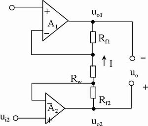
Figure 3Â In-phase parallel differential amplifier
Design Points
Digital phase-locked frequency synthesizer
For a phase-locked synthesizer with high operating frequency and relatively small frequency conversion interval, if the pre-frequency division method is used, the loop frequency division is relatively large. Shifting the frequency down in the feedback branch can effectively reduce the loop frequency division ratio and help improve the phase noise and dynamic response characteristics of the system. This is a commonly used phase-locked synthesizer at present. The working principle is the phase comparison between the reference signal and the feedback signal in the PD . The output voltage is controlled by the loop filter LPF to suppress noise and high-frequency components to control the VCO . The system controls the frequency division ratio of the feedback branch to achieve frequency agility. When the loop is locked, the output frequency is f0=(m+N/p)fi . Its block diagram is shown as in Fig. 2 .
The choice of loop gain: When selecting the loop bandwidth, the loop bandwidth should be much smaller than the loop gain. Therefore, in the design, adding an amplifier between the frequency / phase discriminator and the loop filter will greatly Improve the loop gain, can ensure the improvement of phase noise index. The amplifier circuit is shown as in Fig. 3 .
Because the structure of the in-phase parallel differential amplifier circuit is symmetrical, an external circuit with symmetrical parameters should be selected, that is, Rf1=Rf2=Rf . At this time, the differential mode gain is:
It can be concluded from the above formula that the in-phase parallel differential amplifier can easily adjust the gain only by changing the size of Rw , and the external circuit does not need matching resistance, and the output can obtain a very high common-mode rejection ratio.
Loop bandwidth selection: The power of the phase noise of the voltage-controlled oscillator is mainly concentrated in the low frequency part, and the high-pass filtering effect of the frequency response of the error transfer function of the phase-locked loop is quite significant. At the low frequency end of F < fn , the attenuation increases by 20dB per 10- octave . Based on the above analysis, only in terms of filtering the noise of the voltage-controlled oscillator, fn should be selected as large as possible.
However, the crystal noise of the reference oscillator acts on the input of the loop phase detector, and the loop has a low-pass filter for the crystal noise. The filtering effect depends on the frequency response of the closed-loop transfer function; in the high frequency band of F < fn , -10dB drop every 10 octave . From the above analysis, only in terms of filtering the phase noise of the input crystal oscillator, the smaller the fn of the loop, the better.
In the same coordinate system, first make the phase noise spectrum of the VCO , and then make the phase noise spectrum of the crystal oscillator multiplied by N2 . The intersection of the two spectral lines can be found. As long as the fn of the loop is selected at this intersection frequency, the output phase The noise power is minimal. As long as all the noises are merged into two categories: high-pass and low-pass, the design of the best fn can also be completed using the previous method .
The loop filter adopts an active proportional integral filter, its characteristics are close to the ideal integral filter, there are two independent adjustable parameters, and has a lag - lead characteristic, which is conducive to the stability of the loop.
Based on the DDS chirp signal source
DDS is mainly composed of phase accumulator, sin amplitude converter, D/A converter and low pass filter (LPF) . Its core component is the phase accumulator, as shown in Figure 4. Under the action of the system clock, The phase accumulator completes the frequency accumulation, and uses each accumulation result as the sampling address, periodically scans the sine wave waveform memory, and converts the result into a voltage waveform through the D/A converter.
The relationship among output frequency, frequency control word, and system clock frequency is:
In the formula: FO -the frequency of the output waveform; K -the frequency control word;
FCLK — system clock frequency; N — phase accumulator bit length.
In addition to the main spectrum, the signal synthesized by DDS has a large number of spurious components. These spurious components mainly have three sources. One is caused by phase truncation errors. This can be used to address the phase / amplitude after the phase accumulator output is truncated. The conversion table is measured by the number of bits. The second is that the number of data bits of the waveform memory ROM is limited, which causes the waveform amplitude quantization error. This is determined by the number of output numbers and the number of DACs after phase / amplitude conversion . The third is due to the DAC . Non-ideal characteristics, the step wave produces harmonics and spurious components at the output of the DAC . In this system, the DDS chip uses ADI 's AD9854 as its core, and the spurs caused by phase truncation can be ignored. The quantization error can be based on the actual waveform bandwidth, using oversampling technology and filtering to obtain a higher signal-to-noise ratio. Due to the non-ideal characteristics of DAC , in actual use, only DAC with good linearity can be selected to improve the quality of DDS output signal.
Experimental results
The single-sideband phase noise power spectral density curve (fo=9500MHz) of the local oscillator circuit of the X -band frequency synthesizer completed according to the block diagram shown in Figure 1 is shown in Figure 5 , and the waveform of the linear frequency modulation signal with a bandwidth of 50MHz in the transmitting channel is shown in Figure 6 . .
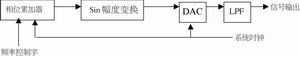
Picture 4Â DDS functional block diagram
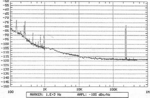
Picture 5Â Single sideband phase noise power spectral density curve
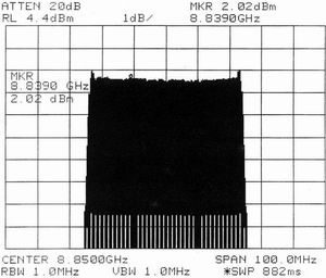
Picture 6Â 50MHz chirp signal waveform
Concluding remarks
Digital integrated phase-locked loop has become the core of indirect frequency synthesizer due to its easy debugging, small size, and low power consumption. DDS has been widely used due to its advantages of wide relative bandwidth, programmable and all-digital structure. Through analysis and system In the verification, this scheme has achieved relatively satisfactory results.
This laminated densified wood is formed through heat pressing after electric industry alkali glass cloth dips into the epoxy phenolic resin. It has high mechanic and dielectric performance, and applicable as insulation structural components for electromechanical/electrical equipment, as well as used under damp environmental conditions and transformer oil.
It is made of alkali-free glass cloth for electrician impregnated with epoxy phenolic resin, baked and hot pressed. The laminate has higher mechanical and electrical properties, better heat resistance and moisture resistance, and has good machinability. The heat resistance level is B level.
Epoxy Board,Fiber Glass Epoxy Board,Epoxy Board Insulation Laminated,Epoxy Fiberglass Cloth Laminated Sheet
Yingkou Dongyuan Electrical Insulation Board Co.,Ltd , https://www.dy-insulation.com